What is a PCB?
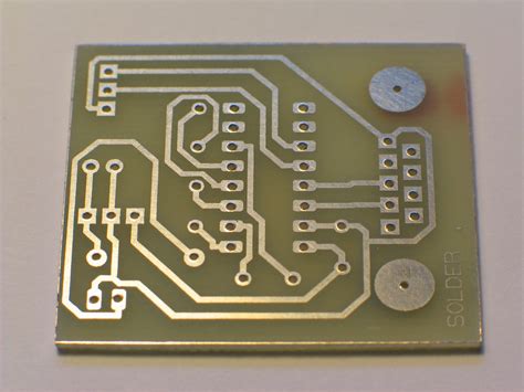
A Printed Circuit Board (PCB) is the foundation of nearly all modern electronic devices. It is a flat board made of insulating material, typically fiberglass or composite epoxy, with conductive pathways printed or etched onto its surface. These pathways, also known as traces, connect various electronic components such as resistors, capacitors, integrated circuits, and more, to create a complete electronic circuit.
PCBs have revolutionized the electronics industry by providing a reliable, compact, and mass-producible means of assembling electronic circuits. They have largely replaced older methods of circuit assembly, such as point-to-point wiring and wire wrap, which were more time-consuming, error-prone, and difficult to mass-produce.
The Importance of PCBs in Electronic Prototyping
In the process of developing a new electronic product, prototyping is a crucial step. It allows designers and engineers to test their circuits, identify and fix issues, and refine their designs before moving to mass production. PCBs play a vital role in this process.
Advantages of Using PCBs for Prototyping
-
Reliability: PCBs provide a stable and reliable platform for electronic circuits. The fixed traces minimize the risk of loose connections and short circuits, which are common issues with breadboards and other prototyping methods.
-
Consistency: PCBs ensure that each prototype is identical, which is crucial for testing and validation. This consistency also makes it easier to transition from prototype to mass production.
-
Compact Size: PCBs allow for much more compact designs compared to other prototyping methods. This is especially important for devices where space is at a premium, such as wearables or IoT devices.
-
Complex Circuits: With the ability to have multiple layers and fine trace widths, PCBs can accommodate complex circuits that would be difficult or impossible to create with other methods.
PCB Prototyping Process
The PCB prototyping process typically involves the following steps:
-
Schematic Design: The circuit is designed using Electronic Design Automation (EDA) software. This includes selecting components, creating the schematic, and running simulations.
-
PCB Layout: Once the schematic is finalized, the physical layout of the PCB is designed. This involves placing components and routing traces, while considering factors such as signal integrity, power delivery, and manufacturability.
-
Fabrication: The designed PCB is then fabricated. For prototypes, this is often done through a PCB prototyping service, which can provide quick-turn, low-volume production.
-
Assembly: The fabricated PCB is populated with components. This can be done by hand for small quantities, or by a pick-and-place machine for larger volumes.
-
Testing and Debugging: The assembled PCB is tested to ensure it functions as intended. Any issues are debugged and the design is refined if necessary.
| Step | Purpose |
|---|---|
| Schematic Design | Create the circuit design |
| PCB Layout | Design the physical layout of the PCB |
| Fabrication | Manufacture the physical PCB |
| Assembly | Populate the PCB with components |
| Testing and Debugging | Verify functionality and fix issues |

Types of PCBs
PCBs come in various types, each with its own characteristics and applications. The main types are:
Single-Layer PCBs
Single-layer PCBs have conductive traces on only one side of the board. They are the simplest and cheapest type of PCB, but they are limited in terms of circuit complexity and density.
Double-Layer PCBs
Double-layer PCBs have conductive traces on both sides of the board. They can accommodate more complex circuits than single-layer PCBs and allow for a more compact design. They are the most common type of PCB.
Multi-Layer PCBs
Multi-layer PCBs have conductive traces on multiple layers, with insulating layers in between. They can have anywhere from 4 to over 100 layers. They are used for very complex circuits and can achieve very high component density.
| PCB Type | Layers | Complexity | Cost |
|---|---|---|---|
| Single-Layer | 1 | Low | Low |
| Double-Layer | 2 | Medium | Medium |
| Multi-Layer | 4+ | High | High |
Flexible PCBs
Flexible PCBs are made from flexible insulating material, allowing them to bend and conform to different shapes. They are used in applications where flexibility is required, such as wearables, medical devices, and aerospace.
Rigid-Flex PCBs
Rigid-flex PCBs are a combination of rigid and flexible PCBs. They have rigid sections for mounting components and flexible sections for connecting these rigid sections. They offer the benefits of both rigid and flexible PCBs.

PCB Materials
The choice of materials for a PCB can significantly impact its performance, reliability, and cost. The main considerations are:
Substrate Material
The substrate is the insulating material that forms the base of the PCB. The most common materials are:
-
FR-4: A composite material made of fiberglass and epoxy resin. It is the most widely used substrate material due to its good mechanical and electrical properties and low cost.
-
High Tg FR-4: A variant of FR-4 with a higher glass transition temperature (Tg), which makes it more heat resistant. It is used in applications with higher operating temperatures.
-
Polyimide: A high-performance polymer that offers excellent heat resistance, chemical stability, and flexibility. It is used in flexible and rigid-flex PCBs.
-
Teflon: A fluoropolymer with very low dielectric constant and loss, making it ideal for high-frequency applications. However, it is expensive and difficult to process.
| Material | Dielectric Constant | Tg (°C) | Applications |
|---|---|---|---|
| FR-4 | 4.2-4.5 | 130-140 | General purpose |
| High Tg FR-4 | 4.2-4.5 | 170-180 | High temperature |
| Polyimide | 3.2-3.6 | 250-400 | Flexible, high temperature |
| Teflon | 2.0-2.1 | 327 | High frequency |
Copper Weight
The copper weight refers to the thickness of the copper layer on the PCB. It is typically expressed in ounces per square foot (oz/ft²), with 1 oz/ft² being about 35 µm thick. Higher copper weights allow for higher current carrying capacity but can make the PCB more expensive and difficult to etch.
Solder Mask
The solder mask is a protective layer applied over the copper traces to prevent accidental short circuits during soldering. It also provides insulation and protection against environmental factors. The most common solder mask colors are green and red, but other colors are available for aesthetic purposes.
Silkscreen
The silkscreen is a layer of text and symbols printed onto the PCB for identification and assembly purposes. It typically includes component designators, company logos, and other markings. The most common silkscreen color is white, but other colors are available.

PCB Design Considerations
Designing a PCB involves balancing many factors to create a product that is functional, reliable, and manufacturable. Some key considerations are:
Signal Integrity
Signal integrity refers to the quality of the electrical signals as they travel through the PCB. Poor signal integrity can lead to issues such as crosstalk, reflections, and electromagnetic interference (EMI). To maintain good signal integrity, designers need to consider factors such as trace width, trace spacing, impedance matching, and ground planes.
Power Delivery
Delivering clean, stable power to all components on the PCB is crucial for proper operation. This involves designing an appropriate power distribution network, which includes power and ground planes, decoupling capacitors, and voltage regulators. The goal is to minimize voltage drop, avoid current crowding, and suppress noise.
Thermal Management
Electronic components generate heat, and this heat needs to be dissipated to prevent overheating and failure. PCB designers need to consider the thermal characteristics of the components and the PCB itself. Techniques for thermal management include using copper pours, thermal vias, and choosing appropriate substrate materials.
Manufacturability
A PCB design is only successful if it can be manufactured reliably and cost-effectively. Designers need to consider the capabilities and limitations of the manufacturing process. This includes factors such as minimum trace width and spacing, hole sizes, and clearances. Following design for manufacturing (DFM) guidelines can help ensure a smooth transition from design to production.
PCB Assembly
Once the PCB is fabricated, it needs to be populated with components to create a functional circuit. The main steps in PCB assembly are:
-
Solder Paste Application: Solder paste, a mixture of tiny solder particles and flux, is applied to the pads on the PCB where components will be placed. This is typically done using a stencil and a squeegee.
-
Component Placement: The components are placed onto the PCB, with their leads or pads aligned with the corresponding pads on the PCB. For prototypes and small volumes, this can be done by hand. For larger volumes, a pick-and-place machine is used.
-
Reflow Soldering: The PCB with the placed components is passed through a reflow oven. The oven heats the PCB, causing the solder paste to melt and then cool, forming a solid electrical and mechanical connection between the components and the PCB.
-
Inspection and Testing: After soldering, the PCB is inspected to ensure all components are properly placed and soldered. Various testing methods, such as in-circuit testing, functional testing, and boundary scan testing, may be used to verify the functionality of the assembled PCB.
Frequently Asked Questions (FAQ)
1. What is the difference between a breadboard and a PCB?
A breadboard is a prototyping tool that allows you to create temporary circuits without soldering. Components are plugged into the holes in the breadboard, and connections are made by metal strips underneath. A PCB, on the other hand, is a permanent circuit board where the components are soldered onto copper traces. PCBs are more reliable, compact, and suitable for mass production, while breadboards are useful for quick prototyping and experimentation.
2. Can I make a PCB at home?
Yes, it is possible to make PCBs at home using methods such as toner transfer or photoresist etching. However, these methods require some skill and equipment, and the quality may not be as good as professionally manufactured PCBs. For most projects, it’s recommended to use a PCB prototyping service, which can provide high-quality PCBs at a reasonable cost and turnaround time.
3. What is the typical turnaround time for PCB prototyping?
The turnaround time for PCB prototyping varies depending on the complexity of the design, the chosen manufacturing service, and shipping times. Many PCB prototyping services offer quick-turn options, which can provide PCBs in as little as 24 hours. However, for standard orders, a typical turnaround time is 1-2 weeks from the time the design files are submitted to the time the PCBs are delivered.
4. How much does it cost to prototype a PCB?
The cost of PCB prototyping depends on factors such as the size of the PCB, the number of layers, the quantity ordered, and the turnaround time. For small, simple PCBs in low quantities, the cost can be as low as a few dollars per board. For larger, more complex boards or higher quantities, the cost can be several hundred dollars or more. Many PCB prototyping services offer online quoting tools that can provide an instant estimate based on your design specifications.
5. What software is used for PCB design?
There are many software tools available for PCB design, ranging from simple, free tools to complex, professional-grade software. Some popular options include:
- KiCad: A free, open-source suite of tools for schematic capture and PCB layout.
- EAGLE: A widely-used, low-cost PCB design software that offers schematic capture, PCB layout, and auto-routing.
- Altium Designer: A high-end, professional PCB design software with advanced features for complex designs.
- OrCAD: A comprehensive PCB design solution that includes schematic capture, simulation, PCB layout, and collaboration tools.
The choice of software depends on factors such as the complexity of your designs, your budget, and your personal preferences.
Conclusion
PCBs are the backbone of modern electronics, and they play a crucial role in the prototyping and development of new electronic products. By understanding the types of PCBs, the materials and processes involved, and the key design considerations, you can create reliable, high-performance prototypes that can be smoothly transitioned into mass production.
Whether you’re a hobbyist working on a personal project or a professional engineer developing a new product, investing time in learning about PCBs and the prototyping process will pay dividends in the quality and success of your electronic designs.
No responses yet