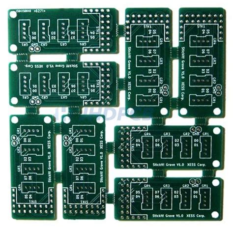
What is PCB Panelization?
PCB panelization is the process of arranging multiple identical or different PCB designs on a single large panel for manufacturing. The main purpose of panelization is to maximize the utilization of the production equipment and minimize the handling of individual boards. By grouping multiple boards together, manufacturers can reduce the time and cost associated with setting up the machines, loading and unloading the panels, and inspecting the finished products.
Benefits of PCB Panelization
- Increased production efficiency
- Reduced manufacturing costs
- Improved material utilization
- Simplified handling and transportation
- Consistent quality across multiple boards
Types of PCB Panelization Methods
There are several PCB panelization methods available, each with its own advantages and disadvantages. The choice of the method depends on factors such as the board size, shape, complexity, and the required level of precision. Let’s explore some of the most common panelization methods.
1. Tab Routing
Tab routing is one of the most popular PCB panelization methods. In this method, small tabs are added to the edges of the individual boards, connecting them to the main panel. These tabs are designed to be easily broken off after the manufacturing process is complete. Tab routing is suitable for boards with simple shapes and moderate sizes.
Advantages:
– Easy to implement
– Suitable for most PCB designs
– Allows for easy separation of individual boards
Disadvantages:
– Not suitable for complex board shapes
– May require additional processing steps to remove the tabs
– Can leave visible marks on the board edges
2. V-Scoring
V-scoring is another common PCB panelization method that involves creating V-shaped grooves along the edges of the individual boards. These grooves are cut partially through the panel, allowing for easy separation of the boards after manufacturing. V-scoring is suitable for boards with straight edges and can provide a clean, smooth edge finish.
Advantages:
– Provides a clean, smooth edge finish
– Suitable for boards with straight edges
– Allows for easy separation of individual boards
Disadvantages:
– Not suitable for complex board shapes
– Requires precise control of the cutting depth to avoid damaging the boards
– May weaken the panel structure if the grooves are too deep
3. Perforated Tabs
Perforated tabs are a variation of the tab routing method, where small perforations are added along the tabs connecting the individual boards to the main panel. These perforations make it easier to break off the tabs after manufacturing, reducing the risk of damaging the boards.
Advantages:
– Easier to separate the boards compared to solid tabs
– Reduces the risk of damaging the boards during separation
– Suitable for most PCB designs
Disadvantages:
– May require additional processing steps to remove the perforated tabs
– Can leave visible marks on the board edges
– Not suitable for complex board shapes
4. Mousebites
Mousebites, also known as nibble holes or break-off tabs, are small circular holes drilled along the edges of the individual boards. These holes create weak points that allow for easy separation of the boards after manufacturing. Mousebites are suitable for boards with complex shapes or tight spacing requirements.
Advantages:
– Suitable for complex board shapes
– Allows for tight spacing between boards
– Provides a clean, smooth edge finish
Disadvantages:
– Requires additional drilling steps during manufacturing
– May weaken the panel structure if the holes are too large or too close together
– Can leave visible marks on the board edges
5. Rail Panelization
Rail panelization involves adding a frame or rail around the perimeter of the panel, with the individual boards connected to the frame using tabs or mousebites. This method provides added stability to the panel and allows for easier handling during manufacturing.
Advantages:
– Provides added stability to the panel
– Allows for easier handling during manufacturing
– Suitable for boards with complex shapes or tight spacing requirements
Disadvantages:
– Requires additional material for the frame or rail
– May increase the overall panel size, reducing material utilization
– Requires additional processing steps to remove the frame or rail after manufacturing

Choosing the Right PCB Panelization Method
When selecting a PCB panelization method, several factors should be considered to ensure the best outcome for your project. These factors include:
-
Board size and shape: The size and shape of the individual boards will influence the choice of the panelization method. Simple shapes and moderate sizes are suitable for tab routing or V-scoring, while complex shapes or tight spacing requirements may require mousebites or rail panelization.
-
Material properties: The properties of the PCB material, such as thickness, flexibility, and brittleness, should be taken into account when choosing a panelization method. Some methods may not be suitable for certain materials or may require additional processing steps to ensure the desired result.
-
Manufacturing capabilities: The available manufacturing equipment and processes will also influence the choice of the panelization method. Some methods may require specialized equipment or additional processing steps, which can impact the overall production time and cost.
-
Cost considerations: The cost of the panelization method should be evaluated in relation to the overall project budget. Some methods may require additional material or processing steps, which can increase the production cost. However, the benefits of panelization, such as increased efficiency and reduced handling, should also be considered when assessing the cost-effectiveness of the chosen method.

PCB Panelization Design Guidelines
To ensure the success of your PCB panelization project, follow these design guidelines:
- Keep the spacing between individual boards consistent and sufficient to allow for the chosen panelization method.
- Ensure that the tabs, grooves, or holes used for panelization are properly sized and positioned to provide adequate strength and ease of separation.
- Consider adding fiducial marks or tooling holes to the panel to aid in the alignment and registration of the boards during manufacturing.
- Include any necessary markings or labels on the panel to assist with the identification and tracking of the individual boards.
- Verify that the panelization design complies with the manufacturing capabilities and requirements of your chosen fabrication partner.

Frequently Asked Questions (FAQ)
-
What is the minimum spacing required between individual boards for PCB panelization?
The minimum spacing between individual boards depends on the chosen panelization method and the manufacturing capabilities of your fabrication partner. Typically, a spacing of 2-5 mm is recommended for most panelization methods, but it is best to consult with your manufacturer for specific guidelines. -
Can different PCB designs be panelized together on the same panel?
Yes, different PCB designs can be panelized together on the same panel, provided that they have similar manufacturing requirements and can be efficiently arranged on the panel. This approach can help to optimize material usage and reduce production costs. -
How does PCB panelization affect the cost of manufacturing?
PCB panelization can help to reduce the overall manufacturing cost by increasing production efficiency, reducing material waste, and simplifying handling and transportation. However, the cost-effectiveness of panelization depends on factors such as the chosen method, the complexity of the board designs, and the manufacturing capabilities of your fabrication partner. -
Can PCB panelization be used for flexible circuits?
Yes, PCB panelization can be used for flexible circuits, but the choice of the panelization method may be limited by the material properties and the required level of flexibility. Tab routing and perforated tabs are commonly used for flexible circuit panelization, but it is important to consult with your manufacturer for specific recommendations. -
What are the most common issues encountered in PCB panelization, and how can they be prevented?
Some of the most common issues encountered in PCB panelization include inadequate spacing between boards, improper sizing or positioning of tabs or holes, and incompatibility with the manufacturing process. These issues can be prevented by following the design guidelines, consulting with your fabrication partner, and ensuring that the panelization design is properly verified and tested before production.
Conclusion
PCB panelization is a valuable technique for optimizing the manufacturing process and reducing production costs in the electronics industry. By understanding the different panelization methods and their advantages and disadvantages, designers and manufacturers can select the most suitable approach for their specific projects. Following the design guidelines and collaborating closely with fabrication partners can help to ensure the success of PCB panelization projects and deliver high-quality, cost-effective products to the market.
No responses yet