What is PCB Panelization?
PCB panelization is the process of arranging multiple printed circuit board designs onto a single panel for manufacturing. By grouping multiple PCBs together, manufacturers can produce boards more efficiently and cost-effectively.
The main goals of PCB panelization are to:
1. Maximize the number of PCBs that can fit on a manufacturing panel
2. Minimize wasted material
3. Ensure the panel remains sturdy and stable during production
4. Allow for easy separation of individual boards after fabrication
Types of PCB Panelization
There are two main methods for panelizing PCBs:
| Method | Description |
|---|---|
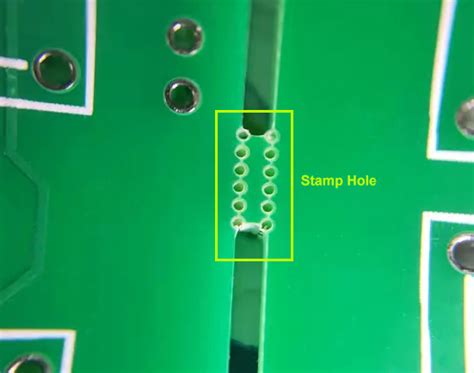
| Tab Routing | Individual boards are connected by tabs or “breakaway mousebites” |
| V-Scoring | Shallow grooves are cut between boards to allow for separation |
Tab routing is the more common method, as it provides a stronger connection between boards during manufacturing. V-scoring can be more economical but requires careful design to ensure the panel remains stable.
Why is PCB Panelization Important?
1. Cost Reduction
One of the primary benefits of panelization is reducing manufacturing costs. By grouping multiple PCBs on a single panel, manufacturers can:
- Minimize setup and handling time
- Reduce wasted material from individually cut boards
- Take advantage of bulk pricing for larger orders
This allows for significant cost savings, especially for high volume production runs. Even for smaller quantities, panelization helps amortize the fixed costs of setting up the manufacturing process.
2. Improved Efficiency
Panelization streamlines the PCB fabrication process by allowing multiple operations to be performed simultaneously on the entire panel, rather than individual boards. This includes:
- Drilling
- Plating
- Solder mask application
- Silkscreen printing
- Surface finish application
By processing the boards in panel form, manufacturers can optimize equipment usage and minimize the number of handling steps required. This improves overall production efficiency and reduces the risk of human error.
3. Enhanced Yield
Effective panelization helps ensure a higher percentage of usable boards from each manufacturing panel. Proper placement and spacing of the individual PCBs allows for maximum utilization of the panel area while maintaining necessary clearances for tooling and handling.
Additionally, well-designed panels are less susceptible to warping or damage during the fabrication process. This reduces the number of rejected boards and improves overall yield.
4. Simplified Assembly
Panelization also offers benefits for the PCB assembly process. Many automated assembly lines are designed to handle standard panel sizes, allowing for efficient placement and soldering of components.
Keeping the boards in panel form during assembly provides a more stable base for the equipment to work with. It also allows for multiple boards to be processed simultaneously, further improving assembly efficiency.
5. Easier Handling and Transport
Panelized PCBs are easier to handle and transport than individual boards. The larger panel size provides more stability and protection during shipping, reducing the risk of damage.
Panels can also be easily stacked and packaged, minimizing the space required for storage and transport. This is particularly important for high volume orders where efficient logistics are critical.
6. Consistent Quality
By processing boards in panel form, manufacturers can ensure more consistent quality across the entire production run. Factors such as plating thickness, solder mask coverage, and hole placement will be more uniform when applied to a larger panel versus individual boards.
Panelization also allows for easier inspection and testing of the boards. Many automated optical inspection (AOI) systems are designed to work with standard panel sizes, enabling quick and accurate quality checks.
7. Design Flexibility
While panelization does impose some constraints on PCB design, it also offers opportunities for flexibility. Designers can incorporate mixed technologies or different board thicknesses within a single panel, as long as they adhere to the manufacturer’s guidelines.
This allows for the production of complex, multi-part assemblies or the combination of different PCB designs to meet specific project requirements. Panelization also enables the use of odd-shaped or non-rectangular boards, as long as they can be efficiently arranged on the panel.
8. Faster Time to Market
By streamlining the manufacturing and assembly processes, panelization helps reduce overall production time for PCBs. This is especially valuable for time-sensitive projects or products with short lifecycles.
Faster production times enable companies to bring their products to market more quickly, providing a competitive advantage. Panelization also allows for more responsive manufacturing, enabling companies to adjust production volumes based on demand.

FAQ
1. What are the standard panel sizes for PCB manufacturing?
Standard panel sizes vary by manufacturer but commonly include:
- 18″ x 24″ (457mm x 610mm)
- 21″ x 24″ (533mm x 610mm)
- 18″ x 21″ (457mm x 533mm)
- 16″ x 18″ (406mm x 457mm)
2. How much space is required between boards on a panel?
The minimum spacing between boards depends on the panelization method and the manufacturer’s capabilities. Typically, a minimum of 0.125″ (3.175mm) is required for tab-routed panels, while v-scored panels may require slightly less.
3. Can different board designs be combined on the same panel?
Yes, different board designs can be panelized together as long as they share the same thickness and material specifications. This is known as a “mixed panel” and can be an effective way to reduce costs for low-volume production.
4. Are there any limitations on board shape for panelization?
In general, most board shapes can be panelized as long as they can be efficiently arranged on the panel. However, highly irregular shapes may require additional spacing or waste more material. It’s best to consult with the manufacturer for specific design guidelines.
5. How are individual boards removed from the panel after fabrication?
For tab-routed panels, the individual boards are typically separated by breaking the tabs manually or with a specialized depaneling tool. V-scored panels are separated by applying pressure along the scoring lines to snap the boards apart. Some manufacturers may offer depaneling as an additional service.

Conclusion
PCB panelization plays a critical role in the efficient and cost-effective manufacturing of printed circuit boards. By understanding the importance of panelization and its impact on the production process, designers and engineers can make informed decisions to optimize their PCB designs for manufacturability.
Effective panelization offers a range of benefits, from cost reduction and improved efficiency to enhanced quality and faster time to market. As PCB technology continues to advance, the ability to effectively panelize designs will remain a key factor in successful electronics manufacturing.

No responses yet