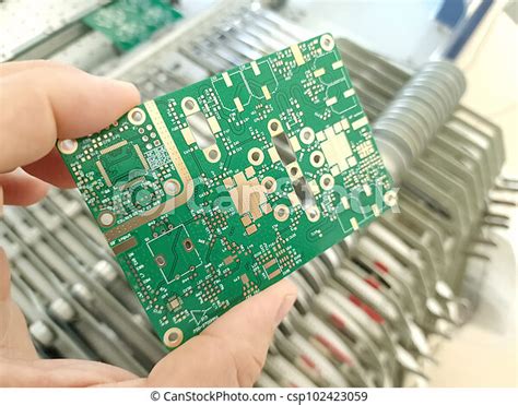
Introduction to RF PCB Assembly
Radio Frequency (RF) and microwave Printed Circuit Board (PCB) assembly is a specialized process that requires careful consideration of various factors to ensure optimal performance and reliability. RF PCB assembly involves the integration of high-frequency components and circuits onto a PCB substrate, which presents unique challenges compared to traditional PCB assembly.
Key Challenges in RF PCB Assembly
- Signal Integrity
- Impedance Matching
- Electromagnetic Interference (EMI)
- Thermal Management
- Component Placement and Routing
Design Considerations for RF PCB Assembly
Material Selection
Choosing the right materials for RF PCB assembly is crucial to ensure high performance and reliability. The following table summarizes common substrate materials used in RF PCB assembly:
| Material | Dielectric Constant | Loss Tangent | Thermal Conductivity (W/mK) | Applications |
|---|---|---|---|---|
| FR-4 | 4.3-4.7 | 0.02 | 0.3 | Low-cost, general-purpose |
| Rogers RO4003C | 3.38 | 0.0027 | 0.71 | High-frequency, low-loss |
| Rogers RO4350B | 3.48 | 0.0037 | 0.69 | High-frequency, low-loss |
| PTFE | 2.1 | 0.0002 | 0.2 | High-frequency, low-loss |
| Ceramic | 9.8-10.2 | 0.0001-0.0005 | 25-200 | High-frequency, high-power |
Impedance Matching
Proper impedance matching is essential to minimize signal reflections and ensure maximum power transfer in RF circuits. The characteristic impedance of a transmission line is determined by its geometry and the dielectric constant of the substrate material. Common impedance values used in RF PCB assembly include:
- 50 ohms: Coaxial cables, connectors, and most RF components
- 75 ohms: Video and cable television applications
- 100 ohms: Differential signaling, such as Ethernet and USB
To achieve the desired impedance, designers must carefully control the width of the signal traces and the thickness of the dielectric layer.
Grounding and Shielding
Effective grounding and shielding techniques are crucial to minimize EMI and ensure signal integrity in RF PCB assembly. Some best practices include:
- Use a solid ground plane to provide a low-impedance return path for high-frequency signals.
- Implement ground stitching vias to connect ground planes on multiple layers and reduce inductance.
- Use guard traces to isolate sensitive signal traces from sources of interference.
- Incorporate shielding enclosures or cans to contain EMI and prevent external interference.
Component Placement and Routing
Proper component placement and routing are critical to minimize signal loss, crosstalk, and EMI in RF PCB assembly. Guidelines for optimal component placement and routing include:
- Place components close to their associated input/output connectors to minimize signal path length.
- Arrange components to minimize crosstalk between adjacent signal traces.
- Use microstrip or stripline transmission lines for controlled impedance routing.
- Avoid sharp bends or discontinuities in signal traces to minimize reflections and signal distortion.
- Implement via fencing or ground shielding to isolate sensitive signals from interference.

Manufacturing Considerations for RF PCB Assembly
Fabrication Techniques
Advanced fabrication techniques are often required to meet the stringent requirements of RF PCB assembly. Some common fabrication techniques include:
- High Density Interconnect (HDI): Enables finer pitch components and higher routing density.
- Buried and blind vias: Allows for more efficient use of PCB real estate and reduces signal path length.
- Controlled impedance: Ensures consistent impedance values along signal traces to minimize reflections.
- Low-loss laminate materials: Reduces signal attenuation and improves overall performance.
Assembly Processes
RF PCB assembly requires specialized processes and equipment to ensure the highest level of precision and reliability. Key assembly processes include:
- Solder paste printing: Applies solder paste to component pads using a stencil or screen.
- Component placement: Places components onto the PCB using automated pick-and-place machines.
- Reflow soldering: Heats the PCB to melt the solder paste and form a permanent connection between components and pads.
- Inspection and testing: Verifies the quality of the assembled PCB using automated optical inspection (AOI), X-ray inspection, and electrical testing.

Testing and Validation of RF PCB Assemblies
RF Performance Testing
Comprehensive testing and validation are essential to ensure that RF PCB assemblies meet the required performance specifications. Common RF performance tests include:
- S-parameter measurements: Measures the reflection and transmission characteristics of the RF circuit.
- Noise figure measurements: Determines the amount of noise introduced by the RF components and circuit.
- Intermodulation distortion (IMD) testing: Assesses the linearity and dynamic range of the RF circuit.
- Electromagnetic compatibility (EMC) testing: Verifies that the RF PCB assembly meets EMI and electromagnetic susceptibility (EMS) requirements.
Reliability Testing
In addition to performance testing, RF PCB assemblies must also undergo reliability testing to ensure long-term durability and functionality. Typical reliability tests include:
- Thermal cycling: Subjects the PCB assembly to alternating high and low-temperature extremes to simulate real-world operating conditions.
- Vibration and shock testing: Evaluates the mechanical integrity of the PCB assembly under dynamic stress conditions.
- Humidity and moisture resistance testing: Assesses the ability of the PCB assembly to withstand exposure to high humidity and moisture levels.
- Accelerated life testing: Applies elevated stress levels to the PCB assembly to predict its long-term reliability and identify potential failure modes.

Frequently Asked Questions (FAQ)
1. What is the difference between RF and microwave frequencies?
RF frequencies typically range from 20 kHz to 300 MHz, while microwave frequencies extend from 300 MHz to 300 GHz. However, the terms are often used interchangeably in the context of PCB assembly.
2. What are the most common RF connectors used in PCB assembly?
Common RF connectors include SMA, SMB, SMC, MMCX, and U.FL. The choice of connector depends on the frequency range, power handling requirements, and mechanical constraints of the application.
3. How can I minimize the impact of parasitic capacitance and inductance in RF PCB assembly?
To minimize parasitic effects, designers should keep signal traces as short as possible, use ground planes to provide a low-impedance return path, and implement proper grounding and shielding techniques.
4. What is the role of via stitching in RF PCB assembly?
Via stitching involves placing multiple vias along a signal trace to connect ground planes on different layers of the PCB. This technique helps to reduce inductance and improve signal integrity in high-frequency circuits.
5. What are the advantages of using low-loss laminate materials in RF PCB assembly?
Low-loss laminate materials, such as Rogers RO4000 series and PTFE, offer several advantages for RF PCB assembly, including lower dielectric loss, higher thermal conductivity, and better-controlled dielectric constant. These properties help to minimize signal attenuation, improve heat dissipation, and ensure consistent performance over a wide frequency range.
Conclusion
RF and Microwave PCB assembly is a complex process that requires careful consideration of design, materials, manufacturing, and testing aspects to ensure optimal performance and reliability. By following best practices in impedance matching, grounding and shielding, component placement and routing, and selecting appropriate materials and fabrication techniques, designers can create high-quality RF PCB assemblies that meet the demanding requirements of modern applications.
As the demand for high-frequency electronics continues to grow, driven by the proliferation of wireless communication, radar, and sensing technologies, the importance of robust RF PCB assembly processes will only increase. By staying up-to-date with the latest design guidelines and manufacturing techniques, engineers and manufacturers can effectively navigate the challenges of RF PCB assembly and deliver innovative solutions for a wide range of industries and applications.
No responses yet