Introduction to Crystal Oscillators in PCB Design
Crystal oscillators are essential components in modern electronic systems, providing a stable and precise frequency reference for various applications such as timing, synchronization, and communication. When designing a printed circuit board (PCB) that incorporates crystal oscillators, it is crucial to follow best practices and guidelines to ensure optimal performance and minimize frequency drift. In this article, we will explore the importance of PCB layout techniques for maintaining steady frequencies with crystal oscillators.
Understanding Crystal Oscillators
What are Crystal Oscillators?
Crystal oscillators are electronic circuits that utilize the piezoelectric properties of a quartz crystal to generate a highly stable and accurate frequency signal. The quartz crystal resonates at a specific frequency when an electric field is applied, and this resonance is used to control the oscillation of the circuit.
Types of Crystal Oscillators
There are several types of crystal oscillators commonly used in electronic systems:
- Simple Crystal Oscillator (XO): A basic oscillator circuit that consists of a quartz crystal and an amplifier.
- Temperature-Compensated Crystal Oscillator (TCXO): Incorporates additional circuitry to compensate for frequency variations caused by temperature changes.
- Oven-Controlled Crystal Oscillator (OCXO): Maintains a stable operating temperature for the crystal using an oven, providing exceptional frequency stability.
- Voltage-Controlled Crystal Oscillator (VCXO): Allows for fine-tuning of the output frequency by varying the voltage applied to the oscillator.
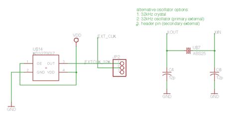
 PCB-layout-Oscillators-8415512ae46711eea457f7f8ca593eb4.jpeg” alt=”” class=”wp-image-136″ srcset=”https://electronicmanufacturingservice.org/wp-content/uploads/2024/03/PCB-Layout-Oscillators-8415512ae46711eea457f7f8ca593eb4.jpeg”>
PCB Layout Considerations for Crystal Oscillators
Placement and Routing
Proper placement and routing of crystal oscillators on the PCB are critical for maintaining stable frequencies. Consider the following guidelines:
- Keep the oscillator close to the load: Place the crystal oscillator as close as possible to the device it is driving, such as a microcontroller or FPGA. This minimizes the length of the traces and reduces the impact of noise and interference.
- Avoid long traces: Keep the traces connecting the crystal oscillator to the load as short as possible. Long traces can introduce unwanted inductance and capacitance, affecting the oscillation frequency.
- Route traces carefully: Ensure that the traces carrying the oscillator signal are routed away from noisy components, such as switching regulators or high-speed digital lines. Avoid running the oscillator traces parallel to these noisy traces to minimize crosstalk.
- Use proper grounding: Provide a solid ground plane near the crystal oscillator and ensure that the ground connections are low-impedance. Use ground vias to connect the oscillator’s ground pins directly to the ground plane.
Decoupling and Filtering
Decoupling and filtering techniques help to reduce noise and maintain a clean power supply for the crystal oscillator. Consider the following:
- Use decoupling capacitors: Place decoupling capacitors, typically in the range of 0.1µF to 10µF, close to the power pins of the crystal oscillator. These capacitors help to filter out high-frequency noise and provide a stable power supply.
- Implement proper power filtering: Use ferrite beads or low-pass filters on the power supply lines to the crystal oscillator. This helps to attenuate high-frequency noise and prevent it from affecting the oscillator’s performance.
Shielding and Isolation
Shielding and isolation techniques can help to minimize the impact of external noise sources on the crystal oscillator. Consider the following:
- Use shielding enclosures: Place the crystal oscillator inside a shielded enclosure or can to protect it from electromagnetic interference (EMI). Ensure that the enclosure is properly grounded to the PCB’s ground plane.
- Isolate the oscillator: If possible, isolate the crystal oscillator from other noisy components on the PCB. This can be achieved by placing the oscillator on a separate PCB layer or using guard rings to create a barrier around the oscillator.
Layout Symmetry and Grounding
Maintaining layout symmetry and proper grounding is important for reducing the impact of parasitic effects on the crystal oscillator. Consider the following:
- Ensure layout symmetry: Design the PCB layout around the crystal oscillator to be as symmetrical as possible. This helps to balance the capacitance and inductance on both sides of the oscillator, minimizing frequency drift.
- Use a solid ground plane: Provide a solid ground plane beneath the crystal oscillator to ensure a low-impedance return path for the oscillator current. Avoid cutting the ground plane near the oscillator, as this can introduce unwanted inductance.

PCB Material Selection
The choice of PCB material can also impact the performance of crystal oscillators. Consider the following factors:
- Dielectric constant: Select a PCB material with a stable dielectric constant over the operating temperature range. Materials with low dielectric constant, such as Rogers RO4000 series, can help to reduce the capacitance and improve the oscillator’s stability.
- Dissipation factor: Choose a PCB material with a low dissipation factor to minimize power loss and maintain a high Q-factor for the oscillator. Materials with low dissipation factors, such as Isola IS400 series, are well-suited for crystal oscillator applications.
- Thermal stability: Opt for PCB materials with good thermal stability to minimize the impact of temperature variations on the oscillator’s frequency. Materials with low thermal expansion coefficients, such as Arlon 25N, can help to reduce frequency drift caused by temperature changes.
Testing and Validation
After implementing the PCB layout guidelines for crystal oscillators, it is essential to perform thorough testing and validation to ensure that the oscillator performs as expected. Consider the following:
- Frequency measurement: Use a frequency counter or oscilloscope to measure the output frequency of the crystal oscillator. Verify that the frequency is within the specified tolerance and remains stable over the operating temperature range.
- Phase noise analysis: Perform Phase noise measurements to assess the spectral purity of the oscillator’s output. Low phase noise is crucial for applications that require high signal-to-noise ratio, such as communication systems.
- Temperature cycling: Subject the PCB to temperature cycling tests to evaluate the stability of the crystal oscillator over the specified temperature range. Monitor the frequency variation and ensure that it remains within acceptable limits.
- EMC testing: Conduct electromagnetic compatibility (EMC) tests to verify that the crystal oscillator does not cause or is not susceptible to electromagnetic interference. This is particularly important for applications that require compliance with regulatory standards.
Frequently Asked Questions (FAQ)
-
What is the purpose of a crystal oscillator in a PCB design?
A crystal oscillator provides a stable and precise frequency reference for timing, synchronization, and communication purposes in electronic systems. -
How does the placement of a crystal oscillator affect its performance?
The placement of a crystal oscillator on the PCB should be as close as possible to the device it is driving, such as a microcontroller or FPGA. This minimizes the length of the traces and reduces the impact of noise and interference. -
What are the benefits of using decoupling capacitors near the crystal oscillator?
Decoupling capacitors placed close to the power pins of the crystal oscillator help to filter out high-frequency noise and provide a stable power supply, ensuring optimal performance of the oscillator. -
How can shielding and isolation techniques improve the stability of a crystal oscillator?
Shielding the crystal oscillator using enclosures or cans helps to protect it from electromagnetic interference (EMI). Isolating the oscillator from noisy components on the PCB using separate layers or guard rings can further minimize the impact of external noise sources. -
What should be considered when selecting PCB materials for crystal oscillator applications?
When selecting PCB materials for crystal oscillator applications, consider factors such as the dielectric constant for reducing capacitance, dissipation factor for minimizing power loss, and thermal stability for reducing frequency drift caused by temperature variations.
Conclusion
Designing a PCB layout that ensures stable and precise frequencies from crystal oscillators requires careful consideration of various factors, including placement, routing, decoupling, filtering, shielding, grounding, and material selection. By following best practices and guidelines, engineers can minimize the impact of noise, interference, and parasitic effects on the oscillator’s performance.
Thorough testing and validation, including frequency measurements, phase noise analysis, temperature cycling, and EMC testing, are essential to verify that the crystal oscillator meets the desired specifications and operates reliably over the intended operating conditions.
By paying attention to these critical aspects of PCB layout for crystal oscillators, designers can create robust and high-performance electronic systems that maintain steady frequencies and deliver accurate timing and synchronization.
No responses yet