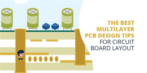
Introduction to Multilayer PCB routing
Printed circuit boards (PCBs) are the backbone of modern electronics. They provide a platform for mounting and interconnecting electronic components to create functional circuits. As electronics have become more complex and miniaturized, multilayer PCBs have become increasingly common.
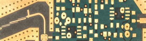
Multilayer PCBs consist of multiple conductive layers separated by insulating dielectric layers. This allows for much higher component density and more complex routing compared to single or double-sided boards. Designing the routing, or interconnections, between components on different layers is a critical aspect of multilayer PCB design.
One key consideration when routing multilayer PCBs is managing the reference planes used for various signals. Let’s dive into what reference planes are, why they are important, and best practices for working with them during multilayer PCB routing.
Understanding Reference Planes in PCB Design
What are PCB reference planes?
A reference plane in a PCB is a large area of copper, typically on an internal layer, that is used as a return path for currents from signals on adjacent layers. The reference plane is usually connected to a power supply or ground.
Having a solid reference plane provides a low-impedance return path for high-frequency signals. This helps maintain signal integrity by minimizing electromagnetic emissions, susceptibility to interference, and crosstalk between signals.
Types of reference planes
The two main types of reference planes used in PCBs are ground planes and power planes:
| Plane Type | Description |
|---|---|
| Ground | Connected to circuit ground, serves as reference for signal layers |
| Power | Carries a specific supply voltage like 3.3V, 5V, etc. |
A PCB may have multiple ground and power planes on different layers, depending on the needs of the circuit. Mixed-signal PCBs often have separate analog and digital ground and power planes to minimize noise coupling.
Role of reference planes in signal integrity
Proper use of reference planes is crucial for maintaining good signal integrity in high-speed PCB designs. A solid reference plane:
- Minimizes loop area between signals and returns, reducing inductance
- Provides shielding between layers to minimize crosstalk
- Acts as a large capacitor to help stabilize power distribution
- Serves as a foundation for controlled impedance routing
Without a low-impedance reference plane nearby, high-speed signals can radiate emissions, couple noise into other signals, and experience significant ringing and reflections due to impedance discontinuities. Careful management of reference planes during routing is essential.

Best Practices for Managing Reference Planes During Routing
Keep signals referenced to a continuous plane
One of the most important rules for routing high-speed signals on a PCB is to always keep them referenced to an unbroken reference plane. If a signal transitions to a new layer, its reference plane should be changed to a plane adjacent to the new signal layer.
Avoid allowing high-speed signals to cross gaps in the reference plane, such as splits or slots. A break in the reference plane disrupts the Return current path, causing large current loops, increased emissions, and degraded signal quality.
If a break in the plane is unavoidable, use a stitching capacitor to bridge the gap at the location where the signal crosses the split. A stitching cap provides a local high-frequency current path to minimize the disruption.
Change reference planes with care
While it’s best for a signal to have a continuous reference along its entire length, this isn’t always possible in complex PCB Stackups. It’s common for signals to need to change reference planes as they are routed between layers.
When a signal does need to change reference planes, it’s important to do so carefully:
- Change reference planes only at a via, never at a trace
- Locate the reference plane change via as close as possible to the signal via
- Place ground vias around the signal via to stitch the two reference planes together
By following these guidelines, the high-frequency return currents from the signal have a direct, low-impedance path to transition between the two reference planes. This minimizes the disruption of the return current and helps preserve signal integrity.
Know when to change reference planes
Changing reference planes at every opportunity is not necessarily best. Excessive reference plane changes can make the return current path more complex and add via stubs that can cause reflections.
In general, only change reference planes when necessary, such as:
- To avoid crossing plane breaks or gaps
- To access a signal layer referenced to a different plane
- To transition between analog and digital sections of the board
Within an area of circuitry, try to route all signals referenced to the same plane if possible. This promotes a simpler current return path and helps keep all the signals in a group referenced to the same supply voltage.
Use stitching vias to tie planes together
Stitching vias are small vias placed along a signal path to stitch its reference planes together at intervals. They provide a low-impedance path for high-frequency return currents to transfer between planes.
Liberal use of stitching vias in high-speed designs can significantly improve signal integrity. Stitching vias help ensure continuous return paths even if a signal briefly transitions to a layer not directly adjacent to its main reference plane.
Some guidelines for using stitching vias:
- Place them at least every λ/4 along the signal path (λ = wavelength of highest significant frequency)
- Use a via size that has minimal impedance at the frequencies of interest
- Locate them as close to the signal vias/traces as possible
- Stitch all relevant reference planes together (e.g. GND to GND, PWR to PWR)
Stitching vias do consume routing space, so use them judiciously. Focus on critical, high-speed signals. Short, low-speed traces may not benefit enough to justify the extra vias.

Power Plane Considerations
Choosing power plane shapes and sizes
The size and shape of power planes in a PCB can have a big impact on power integrity (PI) and electromagnetic compatibility (EMC). Large, unbroken copper pours for power planes are ideal for minimizing impedance and providing good high-frequency bypassing.
However, on dense PCBs it’s often necessary to split up power planes to accommodate signal routing. In this case, try to keep the power plane shapes as large and contiguous as possible. Avoid creating long, thin necks or isolated islands in the plane.
When splitting a power plane, maintain bridges between the sections to keep them tied together:
| Bridging Method | Description |
|---|---|
| Traces | Use wide, short traces between sections |
| Stitching vias | Place vias along the split to stitch sections |
| Copper pours | Pour copper to partially fill in gaps where viable |
The goal is to keep the impedance between the sections of the plane low enough that they function as a single contiguous plane at the frequencies of interest.
Placing power plane bypass capacitors
Bypass (or decoupling) capacitors are critical in a PCB power distribution network (PDN). They provide a local source of charge to help stabilize the supply voltage and shunt high-frequency noise on the power planes.
main considerations when placing bypass caps:
- Locate them as close as possible to the power pins of ICs
- Place multiple values in parallel (e.g. 0.1µF, 0.01µF, 1nF) to cover a wide frequency range
- Orient them to minimize loop inductance (current path from cap to IC and back)
- Provide a direct connection to the power/ground plane pair
A good goal is for every IC to have at least one of each value bypass cap close by. Sensitive or noisy chips like FPGAs, processors, and switching regulators may need many more.
Placing bypass caps on the back side of the PCB can help keep them close to ICs. Use via arrays to provide a low-impedance path from the caps to the inner layer power planes.
Routing Signals Across Plane Breaks
Splitting planes for mixed-signal designs
Mixed-signal PCBs with both analog and digital circuitry often require splitting the ground and power planes to keep the sensitive analog signals isolated from noisy digital currents.
The typical approach is to split the analog and digital ground planes, with a single bridge connecting them at one point near the ADCs/DACs or analog power supplies. This allows the entire PCB to share a common ground reference while minimizing noise coupling between the domains.
Splitting planes like this does complicate signal routing, as now some signals must cross a plane break. Handle these signals with care to avoid compromising signal integrity or allowing noise to couple into sensitive analog nets.
Routing across plane splits
Try to minimize the number of signals that must cross a plane split. Route them on a layer adjacent to a continuous plane if possible. If not, follow these guidelines:
- Place a stitching cap at the split crossing to provide a return path
- Keep the exposed routing over the split as short as possible
- Avoid routing sensitive signals across a split; isolate them to one side
- Use a layer change to cross the split, referenced to planes on both sides
By minimizing the break in the signal’s return path, the degradation in signal integrity can be kept manageable. Simulation tools can help analyze the impact of the split and verify that the routing is robust.
Preventing coupled noise at splits
Plane splits can allow noise to couple between signals referenced to different planes. This is especially concerning for mixed-signal designs, where noisy digital lines might couple into sensitive analog traces at a split.
Some techniques to minimize noise coupling at plane splits include:
- Route critical signals on layers not adjacent to the split
- Keep signals well away from the edges of the split
- Use guard traces or pours referenced to the planes on either side of the split
- Provide high-frequency stitching between the planes at intervals along the split
Guard traces are especially useful for protecting vulnerable analog signals. By providing a conductive barrier referenced to the analog plane, they can help block electric field coupling from signals referenced to the digital plane on the other side of the split.
Conclusion
Managing reference planes is a critical part of routing multilayer PCBs. Proper use of ground and power planes is essential for preserving signal integrity and power integrity in high-speed designs.
By following best practices and carefully planning layer transitions and plane splits, even complex mixed-signal PCBs can have robust routing. Continuous reference planes with stitching vias and bypass capacitors help keep return paths short and direct.
Simulation tools like field solvers and SPICE models are invaluable for analyzing and validating reference plane design decisions. Spending the time to optimize the PCB stackup and reference planes early in the design process can save significant time and expense debugging and respinning boards later.
With the right techniques, changing reference planes during routing can be done effectively to create high-quality, manufacturable PCBs. As signal speeds continue to increase, good reference plane management will only become more critical for successful designs.
FAQ
1. What is the purpose of a PCB reference plane?
A PCB reference plane is a large copper area, usually on an internal layer, that serves as a low-impedance return path for high-frequency signals on nearby layers. It helps maintain signal integrity by minimizing electromagnetic emissions, crosstalk, and susceptibility to interference.
2. Why is it important to avoid crossing gaps in a reference plane?
Crossing a gap or split in a reference plane disrupts the return current path for a signal, forcing the current to take a long, high-impedance detour. This can cause increased emissions, reflections, and signal degradation. It’s best to route signals unbroken reference planes whenever possible.
3. How do you handle unavoidable plane crossings?
If a signal must cross a break in its reference plane, use a stitching capacitor to bridge the gap at the crossing point. A layer change can also allow the signal to transition to a new reference plane. Keep the exposed routing over the gap as short as possible.
4. What is the purpose of stitching vias?
Stitching vias provide a low-impedance interconnection between reference planes on different layers. They allow high-frequency return currents to transfer easily between planes to follow the signal path. Stitching vias are especially useful near plane breaks and signal layer transitions.
5. What types of issues can improper reference plane management cause?
Poor reference plane use can lead to a variety of signal and power integrity problems:
- Excessive radiated emissions and susceptibility to interference
- Increased crosstalk between signals
- Degraded eye diagrams and bit error rates
- Power supply noise, ripple, and pumping
- Resonances and ringing on power planes
- Compromised ESD/EMC compliance
Careful planning and routing with reference planes in mind helps avoid these issues and produce robust PCBs.
No responses yet