What is PCB CAD Software?
PCB CAD (computer-aided design) software is specialized electronic design automation (EDA) tools used to design printed circuit boards (PCBs). PCB CAD programs allow engineers to efficiently plan the layout and routing of electronic components and copper traces on PCBs.
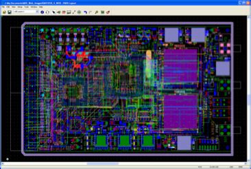
PCB CAD software provides a computer-based method to design the copper traces, component footprints, keepout areas, mounting holes, silkscreen labels, solder masks and other features of a PCB. Modern PCB CAD packages include schematic capture, layout editing, autorouting, design rule checking (DRC), file import/export, and interfaces to manufacturing.
Benefits of Using PCB CAD Software
There are many advantages to using PCB CAD software compared to manual PCB design methods:
- Improved efficiency – PCB CAD tools greatly speed up the design process by automating tedious steps like component placement and routing. What used to take days or weeks can be done in hours with PCB CAD.
- Greater accuracy – PCB CAD enforces design rules and eliminates errors that can occur with manual tape-up or hand-drawn PCB artwork. This improves manufacturing yield.
- Easy revisions – Design changes can be made quickly by editing the CAD database, rather than manually re-drawing the PCB.
–Better documentation – PCB CAD outputs a complete digital model of the board, which serves as the golden reference. Generating fabrication files is automated. - Collaboration – PCB CAD files can be easily shared for peer review or transferred to a manufacturer. Some PCB CAD tools also have real-time collaboration features.
- Simulation and analysis – Many PCB CAD platforms include additional tools for schematic simulation, signal integrity analysis, power analysis, 3D modeling, and more.
In summary, PCB CAD software dramatically improves the productivity and quality of the electronic hardware development process compared to non-computerized methods. PCB CAD is an essential tool for electronics companies developing products with PCBs.
Types of PCB CAD Software
There are two main categories of PCB CAD software:
Desktop PCB CAD
Desktop PCB CAD software runs on a Windows, Mac or Linux PC. The PCB designer interacts with the software via a keyboard, mouse, and computer monitor. Desktop PCB CAD provides a feature-rich environment tailored for the professional PCB designer’s workflow. Schematic capture and board layout are typically done in separate but integrated applications.
Popular desktop PCB CAD software includes:
| Software | Vendor |
|---|---|
| Altium Designer | Altium |
| OrCAD/Allegro | Cadence |
| PADS | Mentor Graphics |
| Xpedition | Mentor Graphics |
| CR-8000 | Zuken |
| DipTrace | Novarm |
Desktop PCB CAD is the most powerful option and is widely used for developing complex, high-density boards. However, it tends to be the most expensive and have the steepest learning curve.
Web-Based PCB CAD
Web-based PCB CAD software runs in a web browser, with the heavy computing done on cloud servers. The user interacts with the software through a browser-based GUI. Schematics and layout are typically done in a unified interface.
Examples of web-based PCB CAD include:
| Software | Vendor |
|---|---|
| EasyEDA | EasyEDA |
| Upverter | Altium |
| CircuitMaker | Altium |
| PCBWeb | Bay Area Circuits |
Advantages of web-based PCB CAD include accessibility from any computer, easier collaboration, and lower cost. The tradeoffs are fewer features and less capacity for large complex designs compared to desktop tools. However, web-based PCB CAD is rapidly evolving and may be sufficient for many users.

Key Features to Look for in PCB CAD Software
When evaluating PCB CAD software, these are some of the most important capabilities to look for:
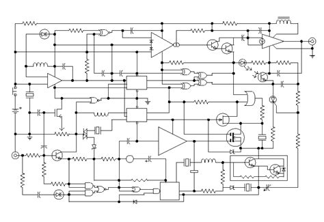
Schematic Capture
- Integrated schematic capture application
- Large library of schematic symbols
- Ability to create custom schematic symbols
- Multi-page and hierarchical schematic support
- Buses and harnesses for connecting multi-signal nets
- Design rule checks for the schematic
Board Layout
- Powerful yet easy-to-use layout and routing tools
- Support for large, fine-pitch BGA and CSP footprints
- Fast, high-completion autorouting with built-in design for manufacturing (DFM) rules
- Real-time, customizable design rule checking
- Integration with mechanical CAD for collision checking
- Comprehensive PCB layer stackup and material library system
- Fast 3D visualization of the board, components and enclosure
Library Management
- Integrated component information system that manages schematic symbols, PCB footprints, 3D models, datasheets, supply chain info, etc.
- Ability to import component data from vendors/suppliers
- Easy tools for creating schematic symbols and PCB footprints
- Verification of footprint-to-schematic mapping
Manufacturing Preparation
- Automatic generation of Gerber, ODB++, IPC-2581 and other PCB fabrication and assembly file formats
- Support for generating 3D PDF, STEP and other 3D CAD formats for enclosure integration
- Customizable PCB documentation generation including drawings, drill files, pick-and-place files, and bill of materials
- Comprehensive design rule checking for manufacturability and electrical functionality
Data Management
- Integrated version control and release management
- Secure access controls for intellectual property protection
- Support for corporate library and design rule standards
- Automated backup and archiving of design databases
- APIs for integration with corporate PLM/ERP/MRP systems
How to Choose a PCB CAD Package
With many PCB CAD options on the market, it can be challenging to select the right one. Consider these factors when making a decision:
-
Design complexity – Make sure the PCB CAD tool has the features and capacity needed for your typical board complexity and manufacturing process. More advanced tools are needed for higher density boards, faster signaling, or challenging manufacturing processes.
-
Ease of use – Look for PCB CAD software with an intuitive interface and good learning resources to flatten the learning curve. This is especially important if PCB design is not a daily a task.
-
Schematic/layout integration – For professional use, you’ll want PCB CAD that includes both schematic capture and layout. The schematic and layout tools should be tightly integrated with cross-probing, ratsnets, ECOs and other features.
-
Library content – Choose PCB CAD that comes with a large library of ready-made schematic symbols, PCB footprints and 3D models. It should be easy to create or import custom parts as well.
-
Manufacturer compatibility – If you plan to outsource PCB fabrication and assembly, ensure that the PCB CAD software generates output files that are compatible with your manufacturing partner. The PCB CAD vendor and manufacturer may have a preexisting relationship to ensure smooth data transfer.
-
Scalability – For a growing organization, consider the upgrade path of the PCB CAD platform. Is it easy to add features, swap parts libraries, increase capacity or add users as your needs grow?
-
Vendor support – Invest in PCB CAD from a vendor with proven stability and responsive technical support. Make sure support resources and training are available in your region and language if needed.
-
Standards certification – Some industries may require that the PCB CAD tool generates output that complies with certain standards, such as IPC-2581 or ITAR. Verify compliance if required.
-
Budget – PCB CAD software ranges in price from free to tens of thousands of dollars. The cost typically scales with capability. Ensure the tool meets your needs but avoid overbuying licenses. Consider the total cost of ownership including subscriptions, support and training.
By methodically reviewing these criteria against the needs of your organization, the field of choices can be narrowed down to a PCB CAD solution that will be a good fit. It’s also important to get buy-in from the actual users of the tool, as they may have strong preferences.
Tips for Learning and Using PCB CAD Software
Becoming proficient with complex PCB CAD software can take time and practice. Here are some tips to make the process easier:
-
Start with tool tutorials – Most PCB CAD tools include built-in tutorials to guide users through the key steps in the design process. Start with these to understand the basic conventions of the tool.
-
Use reference designs – Open and explore reference designs provided by the vendor or user community. Examining professionally created designs is a great way to learn best practices.
-
Leverage vendor training – Take advantage of online webinars, classroom training and user group meetings provided by the PCB CAD vendor. These will help you learn advanced features and pro tips.
-
Consult the user community – Participate in the official user forum for the PCB CAD tool. There you can ask questions, get design feedback, and find downloadable libraries or scripts to automate tasks.
-
Understand key principles – Learn the fundamentals of good PCB design, such as design for manufacturing, grounding, Routing Topologies, layer stackup, and EMI reduction. This knowledge transcends any specific tool.
-
Document corporate standards – Establish and document your company’s schematic, PCB layout and library standards. Configure the tool to enforce those standards, so designers do not have to memorize all the rules.
-
Stay updated – Keep your PCB CAD tool updated with the latest software patches. Periodically review new features to see if they can improve your design process.
With a commitment to continuous learning, PCB designers can keep their skills sharp and fully leverage the powerful features of modern PCB CAD software.
The Future of PCB CAD Software
PCB CAD software vendors continue to introduce new technologies to improve the PCB design process. Here are some of the exciting developments on the horizon:
-
AI assisted routing – Applying machine learning to autorouting algorithms can help complete more of the board faster while following the designer’s preferred routing style.
-
Unsupervised design rule generation – Machine learning can also be used to analyze a company’s past successful designs and automatically generate recommended design rules.
-
AR/VR for design visualization – Virtual and augmented reality interfaces may provide more intuitive ways to arrange the 3D structure of a board and collaborate remotely.
-
MCAD integration – As product development becomes more interdisciplinary, tighter integration is needed between ECAD and MCAD tools. More seamless exchanges of 3D models between the electrical and mechanical domains are needed.
-
Designing with AI – As AI accelerators based on specialized chips and advanced packaging become more common, PCB designers will need tools to take full advantage of this new paradigm.
-Real-time simulation – Expect to see more PCB CAD platforms integrate simulation engines that provide nearly real-time feedback on signal integrity and power integrity, as the design is created.
With the electronic content in all industries growing rapidly, the PCB CAD software segment is seeing heavy investment in R&D. These advanced tools will be key to designing tomorrow’s electronic products.
Frequently Asked Questions (FAQ)
What is the best PCB CAD software?
There is no single “best” PCB CAD tool since the choice depends on the specific needs of the organization. However, some of the most popular PCB CAD platforms for professional use include Altium Designer, Cadence OrCAD/Allegro, Mentor Graphics PADS and Xpedition, and Zuken CR-8000.
How much does PCB CAD software cost?
The cost of PCB CAD software varies widely depending on the type of tool and number of licenses. Entry-level or web-based PCB CAD tools are available for free or for a few hundred dollars. High-end desktop PCB CAD software can cost over $10,000 per license, plus annual subscriptions. Special bundle pricing or subscriptions are usually available for teams and enterprises.
What’s the difference between web based and desktop PCB CAD?
Desktop PCB CAD software is installed and runs locally on a computer, while web-based PCB CAD runs in a web browser with processing done in the cloud. Desktop PCB CAD tends to have more features and be better suited for large, complex designs. Web-based PCB CAD is more affordable, accessible and easier to use, but may have limitations for advanced designs.
Will PCB CAD software replace PCB designers?
No. While PCB CAD automates many tedious steps in the design process, it still requires the knowledge and guidance of skilled PCB designers. PCB designers play a critical role in defining constraints, optimizing performance, creatively arranging the board, and ensuring manufacturability. As AI-driven automation advances, the role of the PCB designer will shift to more of a high-level architecture and supervisory role. But the need for experienced PCB designers will remain.
What skills are needed to be a PCB designer?
To be a successful PCB designer, a combination of technical and soft skills are required:
- Electrical engineering fundamentals
- An understanding of electronic components and manufacturing processes
- Experience with schematic capture, PCB layout and simulation tools
- Knowledge of industry standards and design for manufacturing
- Problem solving and attention to detail
- Ability to manage multiple projects and deadlines
- Communication skills to interface with colleagues and suppliers
- Continuous learning to keep up with new technologies
Larger organizations may have specialized roles for schematic capture, PCB layout, signal integrity, and library management. But in smaller teams, the PCB designer may be responsible for the entire flow from concept to manufacturing hand-off. The PCB designer plays a key role in bringing electronic products to life.
Conclusion
PCB CAD software has revolutionized the way we design printed circuit boards. It has made the process faster, more accurate, and more efficient than ever before. When selecting PCB CAD tools, organizations must carefully consider their current and future needs in terms of design complexity, team size, ease of use, manufacturability, and cost.
By leveraging the latest advancements in PCB CAD technology such as integration with simulation, MCAD collaboration and AI automation, designers can create more complex and reliable electronic products in less time. The role of the PCB designer continues to evolve, requiring a blend of technical and interpersonal skills.
As PCBs remain at the heart of the ongoing electronics revolution across all industries, PCB CAD software will be an indispensable tool for years to come. Exciting developments in automation, visualization and integration will make tomorrow’s PCB CAD platforms even more capable. Investing in the right PCB CAD solution and building a team of skilled PCB designers is a strategic imperative for any organization developing electronic products.
No responses yet