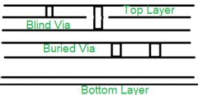
What is a Blind Via?
A blind via is a type of interconnect that connects an outer layer to one or more inner layers of a PCB, without penetrating through the entire board. Unlike through-hole vias, which are visible on both sides of the PCB, blind vias are only visible on one side of the board. This unique characteristic allows for more efficient use of space and enables the creation of high-density PCB designs.
Advantages of Blind Vias
- Space-saving: Blind vias allow for more components to be placed on a smaller PCB surface area, reducing the overall size of the device.
- Improved signal integrity: By reducing the distance between layers, blind vias minimize signal loss and improve overall signal integrity.
- Enhanced thermal management: Blind vias can be used to dissipate heat more effectively, leading to better thermal management in high-power applications.
- Increased design flexibility: Designers can create more complex and compact layouts by utilizing blind vias in their PCB designs.
Manufacturing Process of Blind Vias
The manufacturing process of blind vias involves several steps that ensure the creation of high-quality interconnects. The most common methods for creating blind vias include:
Mechanical Drilling
Mechanical drilling is the traditional method for creating blind vias. In this process, a precise drill bit is used to create holes that partially penetrate the PCB. The depth of the hole is carefully controlled to ensure that it reaches the desired inner layer without penetrating through the entire board.
Laser Drilling
Laser drilling has gained popularity in recent years due to its ability to create smaller and more precise blind vias. In this process, a high-powered laser is used to vaporize the dielectric material, creating a clean and accurate hole. Laser drilling is particularly useful for creating micro vias, which are essential for high-density PCB designs.

Design Considerations for Blind Via PCBs
When designing a PCB with blind vias, several factors must be taken into consideration to ensure optimal performance and manufacturability:
Via Size and Aspect Ratio
The size of the blind via and its aspect ratio (the ratio of the via’s depth to its diameter) are crucial factors in determining the manufacturability and reliability of the PCB. As a general rule, the aspect ratio should be kept below 1:1 to ensure proper plating and to avoid issues such as voids or incomplete filling.
| Via Diameter (mm) | Maximum Depth (mm) | Aspect Ratio |
|---|---|---|
| 0.2 | 0.2 | 1:1 |
| 0.3 | 0.3 | 1:1 |
| 0.4 | 0.4 | 1:1 |
| 0.5 | 0.5 | 1:1 |
Pad Size and Clearance
The pad size and clearance around the blind via must be carefully designed to ensure proper connection and to avoid any potential short circuits. The pad size should be large enough to accommodate the via and provide sufficient space for the plating process. The clearance between the via and adjacent traces or components should also be adequate to prevent any unintended connections.
Layer Stack-up
The layer stack-up of the PCB plays a significant role in the design of blind vias. The number of layers, their arrangement, and the dielectric material used will determine the feasibility and performance of the blind vias. It is essential to work closely with the PCB manufacturer to ensure that the layer stack-up is optimized for the specific requirements of the design.

Blind Via Placement Strategies
The placement of blind vias on a PCB is a critical aspect of the design process. Proper placement can help minimize signal integrity issues, improve manufacturability, and reduce costs. Some key strategies for blind via placement include:
Signal Integrity Optimization
Blind vias should be placed in a way that minimizes the distance between the via and the components it connects. This helps reduce signal loss and improve overall signal integrity. Additionally, it is important to consider the routing of traces around the blind vias to avoid any potential signal integrity issues.
Manufacturing Optimization
To optimize the manufacturing process, blind vias should be placed in areas that are easily accessible for drilling and plating. This means avoiding placement near the edges of the board or in areas with high component density. It is also important to consider the aspect ratio and the spacing between vias to ensure reliable manufacturing.
Cost Optimization
The cost of manufacturing blind via PCBs can be significantly higher than traditional through-hole PCBs. To optimize costs, designers should consider the minimum number of blind vias required for the design and place them strategically to minimize the overall count. Additionally, using standardized via sizes and placement patterns can help reduce tooling costs and improve manufacturing efficiency.

Testing and Quality Control
Ensuring the quality and reliability of blind via PCBs requires rigorous testing and quality control measures. Some of the key testing methods include:
Continuity Testing
Continuity testing is performed to ensure that the blind vias are properly connected to the intended layers and that there are no open circuits. This can be done using a multimeter or a dedicated continuity tester.
Impedance Testing
Impedance testing is used to verify that the impedance of the blind vias matches the designed value. This is crucial for maintaining signal integrity and ensuring proper functioning of the circuit.
Cross-sectioning
Cross-sectioning involves cutting the PCB along the blind via and examining the cross-section under a microscope. This allows for visual inspection of the via’s plating quality, filling, and any potential defects.
Applications of Blind Via PCBs
Blind via PCBs find applications in a wide range of industries and products, including:
- Smartphones and tablets
- Wearable devices
- Medical devices
- Automotive electronics
- Aerospace and defense systems
- High-performance computing
- IoT devices
The compact size, improved signal integrity, and enhanced thermal management offered by blind via PCBs make them ideal for these applications, where space is limited, and performance is critical.
Frequently Asked Questions (FAQ)
-
Q: What is the difference between a blind via and a buried via?
A: A blind via connects an outer layer to one or more inner layers, without penetrating through the entire board. A buried via, on the other hand, connects two or more inner layers without being visible on either side of the PCB. -
Q: Can blind vias be used in multi-layer PCBs?
A: Yes, blind vias are commonly used in multi-layer PCBs to connect the outer layers to the inner layers. This allows for more efficient use of space and enables the creation of high-density PCB designs. -
Q: What are the challenges associated with manufacturing blind via PCBs?
A: The main challenges in manufacturing blind via PCBs include maintaining the proper aspect ratio, ensuring complete plating of the via, and avoiding defects such as voids or incomplete filling. Additionally, the cost of manufacturing blind via PCBs can be higher compared to traditional through-hole PCBs. -
Q: How can I ensure the reliability of blind vias in my PCB design?
A: To ensure the reliability of blind vias, consider factors such as via size, aspect ratio, pad size, and clearance during the design phase. Work closely with your PCB manufacturer to optimize the layer stack-up and follow best practices for via placement. Conduct thorough testing and quality control measures to identify and address any potential issues. -
Q: Are there any limitations to using blind vias in PCB design?
A: The main limitations of using blind vias include the increased manufacturing cost and the need for specialized equipment and processes. Additionally, the aspect ratio of blind vias must be carefully controlled to ensure proper plating and avoid manufacturing defects. Designers must also consider the impact of blind vias on signal integrity and thermal management when creating high-density PCB layouts.
Conclusion
Blind via PCBs have become an essential component in modern electronic devices, offering numerous advantages such as space savings, improved signal integrity, and enhanced thermal management. By understanding the seven key elements discussed in this article, including the manufacturing process, design considerations, placement strategies, testing, and applications, you can effectively incorporate blind vias into your PCB designs.
As technology continues to advance, the demand for more compact and high-performance electronic devices will only increase. Blind via PCBs will play a crucial role in meeting these demands, enabling the creation of innovative and efficient products across various industries.
When designing a PCB with blind vias, it is essential to work closely with experienced PCB manufacturers who have the expertise and capabilities to handle the unique challenges associated with blind via fabrication. By collaborating with the right partners and following best practices for design and manufacturing, you can unlock the full potential of blind via PCBs and create cutting-edge electronic devices that meet the demands of the future.
No responses yet