Introduction to Signal Integrity in RF/Microwave PCBs
Signal integrity is a critical aspect of designing and manufacturing high-performance printed circuit boards (PCBs) for RF and microwave applications. As the demand for faster data rates, higher frequencies, and more compact devices continues to grow, maintaining signal integrity becomes increasingly challenging. Signal integrity issues can lead to degraded performance, increased bit error rates, and even complete system failure.
In multilayer PCBs, the complexity of Signal Integrity Optimization is further compounded by the presence of multiple layers, vias, and interconnects. These elements introduce additional sources of signal distortion, crosstalk, and losses that must be carefully managed to ensure reliable operation.
This article delves into the key concepts and techniques for optimizing signal integrity in RF/microwave transmission lines within multilayer PCBs. We will explore the fundamental principles of signal propagation, the impact of PCB materials and geometry, and the various strategies for mitigating signal integrity issues.
Understanding Signal Propagation in Transmission Lines
Transmission Line Theory
Transmission line theory is the foundation for understanding signal propagation in RF/microwave PCBs. A transmission line is a medium that guides electromagnetic waves from one point to another with minimal loss and distortion. In PCBs, transmission lines are typically realized as microstrip or stripline structures.
The characteristic impedance (Z₀) of a transmission line is a critical parameter that determines how signals propagate along the line. It is defined as the ratio of the voltage to the current for a wave traveling in one direction. For optimal signal integrity, the characteristic impedance should be matched to the source and load impedances to minimize reflections and standing waves.
The propagation velocity (v) of a signal along a transmission line is determined by the dielectric constant (εᵣ) of the surrounding medium. In PCBs, the dielectric constant of the substrate material plays a significant role in determining the signal speed. The relationship between propagation velocity and dielectric constant is given by:
v = c / √εᵣ
where c is the speed of light in vacuum (approximately 3 × 10⁸ m/s).
Impedance Matching
Impedance matching is essential for ensuring efficient power transfer and minimizing signal reflections at the interfaces between the source, transmission line, and load. When there is an impedance mismatch, a portion of the signal energy is reflected back towards the source, leading to signal distortion and degraded performance.
To achieve impedance matching, designers must carefully select the dimensions and materials of the transmission line to achieve the desired characteristic impedance. The characteristic impedance of a microstrip line, for example, is determined by the width of the trace (W), the thickness of the substrate (H), and the dielectric constant of the substrate material (εᵣ).
There are various techniques for impedance matching, including:
-
Stub Matching: This involves adding a short or open-circuited transmission line (stub) at a specific distance from the load to cancel out reflections.
-
Tapered Matching: Gradually changing the dimensions of the transmission line to transition from one impedance to another.
-
Lumped Element Matching: Using discrete components such as capacitors and inductors to match impedances.
Losses in Transmission Lines
Transmission lines exhibit various types of losses that can degrade signal integrity. The main types of losses are:
-
Conductor Losses: Caused by the resistance of the metal traces, which increases with frequency due to the skin effect.
-
Dielectric Losses: Resulting from the dissipation of energy in the substrate material, which is frequency-dependent.
-
Radiation Losses: Occurring when energy is radiated away from the transmission line, particularly at discontinuities and bends.
To minimize losses, designers can:
- Use low-loss substrate materials with a low dissipation factor (tanδ).
- Increase the thickness of the metal traces to reduce conductor losses.
- Minimize discontinuities and abrupt changes in the transmission line geometry.
- Use smooth bends instead of sharp corners to reduce radiation losses.

Impact of PCB Materials on Signal Integrity
Substrate Materials
The choice of substrate material is critical for maintaining signal integrity in RF/microwave PCBs. The substrate acts as the dielectric medium through which the signals propagate, and its properties significantly influence the transmission line characteristics.
Some common substrate materials used in RF/microwave PCBs include:
-
FR-4: A low-cost, flame-retardant epoxy laminate that is widely used in general-purpose PCBs. However, its relatively high dielectric constant and dissipation factor make it less suitable for high-frequency applications.
-
Rogers Materials: High-performance materials specifically designed for RF/microwave applications, such as RO4003C, RO4350B, and RT/duroid 5880. These materials offer low dielectric constant, low dissipation factor, and excellent thermal stability.
-
PTFE (Teflon): A low-loss material with a very low dielectric constant and dissipation factor, making it ideal for high-frequency applications. However, it is more expensive and challenging to process compared to other materials.
When selecting a substrate material, designers must consider factors such as the dielectric constant, dissipation factor, thermal stability, and cost. The table below compares the properties of some common substrate materials:
| Material | Dielectric Constant (εᵣ) | Dissipation Factor (tanδ) |
|---|---|---|
| FR-4 | 4.3 – 4.7 | 0.02 – 0.03 |
| RO4003C | 3.38 | 0.0027 |
| RO4350B | 3.48 | 0.0037 |
| RT/duroid 5880 | 2.20 | 0.0009 |
Copper Thickness and Surface Roughness
The thickness and surface roughness of the copper traces on the PCB also play a role in signal integrity. Thicker copper traces have lower resistance and can handle higher current densities, reducing conductor losses. However, thicker traces also increase the overall thickness of the PCB, which can affect the characteristic impedance of the transmission lines.
Surface roughness can impact signal integrity by increasing conductor losses and affecting the adhesion between the copper and the substrate. Rougher surfaces have a larger surface area, which increases the skin effect and leads to higher losses at high frequencies. Smooth copper surfaces, achieved through processes such as electrolytic copper plating or rolled copper foil, can help minimize these losses.

PCB Geometry and Layout Considerations
Microstrip and Stripline Structures
Microstrip and stripline are two common transmission line structures used in RF/microwave PCBs. The choice between these structures depends on factors such as the desired characteristic impedance, the available board space, and the required isolation between signals.
Microstrip consists of a conductive trace on one side of the substrate, with a ground plane on the opposite side. The characteristic impedance of a microstrip line is determined by the width of the trace, the thickness of the substrate, and the dielectric constant of the substrate material. Microstrip is easier to fabricate and allows for simpler component placement, but it is more susceptible to electromagnetic interference (EMI) and has higher radiation losses compared to stripline.
Stripline, on the other hand, consists of a conductive trace embedded between two ground planes within the substrate. The characteristic impedance of a stripline is determined by the width of the trace, the distance between the ground planes, and the dielectric constant of the substrate material. Stripline offers better isolation and lower radiation losses compared to microstrip, but it requires more layers and is more challenging to fabricate and route.
Vias and Interconnects
Vias and interconnects are essential for connecting signals between different layers in a multilayer PCB. However, they can also introduce discontinuities and impedance mismatches that can degrade signal integrity.
Through-hole vias are the most common type of via, where a hole is drilled through the entire thickness of the PCB and plated with conductive material. Through-hole vias can introduce significant inductance and capacitance, which can cause impedance mismatches and reflections. To minimize these effects, designers can use techniques such as via stitching (placing vias close together to reduce inductance) or back-drilling (removing the unused portion of the via to reduce stub effects).
Blind and buried vias are used to connect inner layers of the PCB without going through the entire board thickness. These types of vias offer more flexibility in routing and can help reduce the overall board size. However, they are more expensive to fabricate and can still introduce discontinuities if not designed properly.
Signal Routing and Trace Geometry
Proper signal routing and trace geometry are critical for maintaining signal integrity in RF/microwave PCBs. Some key considerations include:
-
Trace Width: The width of the traces should be carefully chosen to achieve the desired characteristic impedance while minimizing losses. Wider traces have lower resistance but may not always be feasible due to space constraints.
-
Trace Spacing: Adequate spacing between traces is necessary to minimize crosstalk and coupling between adjacent signals. The spacing should be based on the signal frequencies, rise times, and tolerable crosstalk levels.
-
Bends and Corners: Sharp bends and corners in traces can cause reflections and radiation losses. To minimize these effects, designers should use smooth bends with a large radius or chamfered corners.
-
Length Matching: For critical signals, such as clock lines or differential pairs, the lengths of the traces should be matched to ensure proper timing and phase alignment. Length matching can be achieved through techniques such as serpentine routing or delay lines.

Strategies for Signal Integrity Optimization
Simulation and Modeling
Simulation and modeling tools are essential for optimizing signal integrity in RF/microwave PCBs. These tools allow designers to analyze the behavior of transmission lines, predict signal distortions, and evaluate the impact of different design choices.
Electromagnetic (EM) simulation tools, such as Ansys HFSS or Keysight ADS, can accurately model the electromagnetic fields and wave propagation in complex PCB structures. These tools can help designers optimize the transmission line geometry, evaluate the impact of discontinuities, and estimate losses and coupling.
Circuit simulation tools, such as Cadence Spectre or Keysight ADS, can be used to analyze the overall system performance, including the effects of terminations, matching networks, and component parasitics. Circuit simulations can help designers optimize the impedance matching, evaluate the impact of losses, and verify the system-level performance.
Grounding and Shielding
Proper grounding and shielding techniques are essential for minimizing EMI, reducing crosstalk, and improving signal integrity in RF/microwave PCBs.
Ground planes provide a low-impedance return path for signals and help to minimize the loop area of current flows. In multilayer PCBs, ground planes should be placed close to the signal layers to reduce the inductance of the return path. Stitching vias can be used to connect ground planes on different layers, creating a continuous ground reference.
Shielding involves enclosing sensitive signals or components within a conductive barrier to prevent interference from external sources. Shielding can be achieved through techniques such as:
-
Coplanar waveguide (CPW): A transmission line structure that consists of a signal trace with ground planes on either side, providing built-in shielding.
-
Grounded coplanar waveguide (GCPW): Similar to CPW, but with additional ground planes above and below the signal layer, offering even better shielding.
-
Shielding cans: Metal enclosures that can be placed over sensitive components or regions of the PCB to provide localized shielding.
Power Distribution Network (PDN) Optimization
The power distribution network (PDN) plays a critical role in maintaining signal integrity by providing a stable and low-impedance power supply to the active components on the PCB. A poorly designed PDN can lead to voltage fluctuations, noise coupling, and signal distortion.
To optimize the PDN, designers should:
-
Use decoupling capacitors: Place decoupling capacitors close to the power pins of active components to provide a local, low-impedance source of charge and minimize voltage fluctuations.
-
Minimize PDN impedance: Use wide power and ground planes, multiple vias, and a proper layer stackup to minimize the impedance of the PDN over a wide frequency range.
-
Avoid resonances: Carefully choose the values and placement of decoupling capacitors to avoid creating resonances in the PDN impedance profile.
-
Use power plane segmentation: Divide the power plane into separate segments for different supply voltages or noise-sensitive circuits to minimize coupling and interference.
Manufacturing Considerations
Signal integrity optimization does not end with the design phase; it is also essential to consider manufacturing aspects to ensure the PCB performs as intended.
Fabrication tolerances: PCB manufacturers have certain tolerances for parameters such as trace width, spacing, and dielectric thickness. Designers must account for these tolerances in their simulations and design rules to ensure the manufactured board meets the required specifications.
Material selection: Choosing the right materials for the PCB stackup is crucial for achieving the desired electrical properties and maintaining signal integrity. Designers should work closely with the PCB manufacturer to select materials that are compatible with the fabrication process and meet the performance requirements.
Testing and validation: After fabrication, it is important to perform thorough testing and validation of the PCB to verify its signal integrity performance. This can include techniques such as:
-
Time-domain reflectometry (TDR): Measuring the impedance profile of transmission lines and identifying discontinuities or mismatches.
-
Vector network analyzer (VNA) measurements: Characterizing the S-parameters of the PCB and comparing them with the simulated results to validate the design.
-
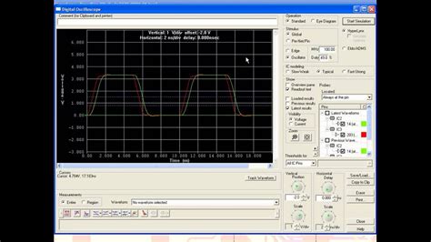
Eye diagram analysis: Evaluating the quality of high-speed digital signals by measuring parameters such as eye height, eye width, and jitter.
Conclusion
Signal integrity optimization is a critical aspect of designing and manufacturing high-performance RF/microwave PCBs. By understanding the principles of signal propagation, the impact of PCB materials and geometry, and the various strategies for mitigating signal integrity issues, designers can create robust and reliable PCBs that meet the ever-increasing demands of modern electronic systems.
Some key takeaways from this article include:
-
Transmission line theory and impedance matching are fundamental concepts for ensuring efficient signal propagation and minimizing reflections.
-
The choice of substrate materials, copper thickness, and surface roughness can significantly impact signal integrity.
-
Proper PCB geometry, including the use of microstrip or stripline structures, vias, and trace routing, is essential for maintaining signal integrity.
-
Simulation and modeling tools are invaluable for optimizing signal integrity and evaluating the impact of design choices.
-
Grounding, shielding, and PDN optimization techniques are crucial for minimizing EMI, reducing crosstalk, and providing a stable power supply.
-
Manufacturing considerations, such as fabrication tolerances, material selection, and testing, are essential for ensuring the PCB performs as intended.
By following these guidelines and best practices, designers can create RF/microwave PCBs with optimized signal integrity, enabling the development of high-performance electronic systems across a wide range of applications, from wireless communications to radar and sensing.
Frequently Asked Questions (FAQ)
-
What is signal integrity, and why is it important in RF/microwave PCBs?
Signal integrity refers to the ability of a signal to propagate through a transmission line with minimal distortion, loss, and interference. In RF/microwave PCBs, maintaining signal integrity is crucial for ensuring the proper functioning of high-frequency circuits, minimizing bit error rates, and achieving the desired system performance. -
What are the main factors that affect signal integrity in multilayer PCBs?
Several factors can affect signal integrity in multilayer PCBs, including: - PCB material properties, such as dielectric constant and dissipation factor
- Transmission line geometry, including trace width, spacing, and routing
- Discontinuities and impedance mismatches caused by vias, connectors, and component placement
- Electromagnetic interference (EMI) and crosstalk from adjacent signals
-
Power distribution network (PDN) impedance and noise
-
How can I select the right substrate material for my RF/microwave PCB?
When selecting a substrate material for an RF/microwave PCB, consider factors such as the dielectric constant, dissipation factor, thermal stability, and cost. Low-loss materials with a low dielectric constant and dissipation factor, such as Rogers RO4000 series or RT/duroid, are often preferred for high-frequency applications. However, the choice ultimately depends on the specific requirements of your design, such as the frequency range, power handling, and environmental conditions. -
What are some common techniques for optimizing signal integrity in RF/microwave PCBs?
Some common techniques for optimizing signal integrity in RF/microwave PCBs include: - Using appropriate transmission line structures, such as microstrip or stripline, based on the design requirements
- Ensuring proper impedance matching and termination to minimize reflections
- Optimizing trace geometry, including width, spacing, and routing, to minimize losses and crosstalk
- Implementing effective grounding and shielding strategies to reduce EMI and improve signal isolation
- Optimizing the power distribution network (PDN) to provide a stable and low-impedance power supply
- Using simulation an
No responses yet