Understanding the Basics of Multilayer PCB Design
Before diving into specific PCB layout tips, it’s crucial to understand the fundamentals of multilayer PCB design. A multilayer PCB consists of multiple conductive layers separated by insulating layers, allowing for higher component density and more complex routing compared to single-layer or double-layer boards.
Advantages of Multilayer PCBs
| Advantage | Description |
|---|---|
| Increased component density | Multilayer PCBs allow for more components to be placed on a smaller board size |
| Improved signal integrity | Proper layer stacking and routing techniques can minimize crosstalk and electromagnetic interference (EMI) |
| Enhanced thermal management | Dedicated power and ground planes help dissipate heat more effectively |
| Reduced electromagnetic interference | Proper grounding and shielding techniques can minimize EMI emissions |
Planning Your Multilayer PCB Layout
Careful planning is essential for a successful multilayer PCB design. Consider the following factors before starting your layout:
Determine the Number of Layers
The number of layers in your multilayer PCB will depend on the complexity of your circuit, the number of components, and the signal integrity requirements. A typical multilayer PCB can have 4, 6, 8, or more layers. Here’s a common layer stackup for a 6-layer board:
| Layer | Purpose |
|---|---|
| Top | Signal |
| Ground | Ground plane |
| Inner 1 | Signal |
| Inner 2 | Signal |
| Power | Power plane |
| Bottom | Signal |
Define the Board Size and Shape
Determine the physical dimensions and shape of your PCB based on the enclosure or space constraints of your product. Consider component placement and routing space when selecting the board size.
Create a Component Placement Plan
Arrange components on the PCB in a logical manner, considering signal flow, power distribution, and thermal management. Place components that interact with each other close together to minimize trace lengths and reduce signal integrity issues.
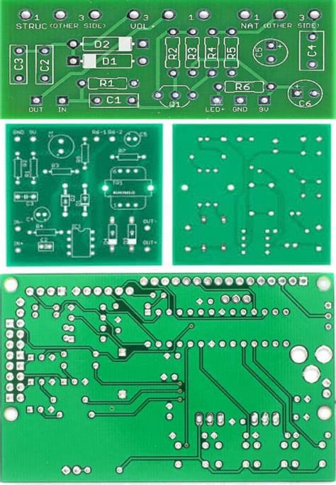
 PCB-layout-Tips-0547d268e44011ee83d5f7f8ca593eb4.jpeg” alt=”” class=”wp-image-136″ srcset=”https://electronicmanufacturingservice.org/wp-content/uploads/2024/03/PCB-Layout-Tips-0547d268e44011ee83d5f7f8ca593eb4.jpeg”>
Signal Integrity and EMI Reduction Techniques
Maintaining signal integrity and minimizing electromagnetic interference are critical aspects of multilayer PCB design. Here are some tips to help you achieve these goals:
Use Proper Layer Stacking
Arrange your layers to minimize crosstalk and EMI. Place signal layers adjacent to ground or power planes to provide shielding and reduce crosstalk. Alternate signal layers with ground and power planes to create a balanced stackup.
Implement Controlled Impedance Routing
Use controlled impedance routing techniques to maintain consistent trace impedance and minimize signal reflections. This involves calculating trace widths and spacing based on the desired characteristic impedance and the dielectric properties of the PCB material.
Minimize Via Count and Size
Vias introduce discontinuities in signal paths and can affect signal integrity. Minimize the number of vias in your design and use small via sizes to reduce capacitance and inductance effects. Use blind and buried vias when necessary to optimize signal routing.
Route High-Speed Signals with Care
High-speed signals require special attention to maintain signal integrity. Follow these guidelines when routing high-speed traces:
- Keep high-speed traces as short as possible
- Avoid sharp corners and use smooth curves for trace routing
- Maintain consistent trace widths and spacing
- Provide ground shielding for critical high-speed signals

Power Distribution and Grounding Strategies
Proper power distribution and grounding are essential for the stable operation of your multilayer PCB. Consider these tips:
Use Dedicated Power and Ground Planes
Assign dedicated layers for power and ground planes to provide low-impedance paths for power distribution and current return. This helps minimize voltage drops and reduces noise coupling between signals.
Implement Proper Decoupling
Place decoupling capacitors close to power pins of ICs to minimize power supply noise and provide a stable voltage reference. Use a combination of bulk, ceramic, and tantalum capacitors to cover different frequency ranges.
Optimize Ground Plane Connections
Provide multiple ground connections for components and connectors to minimize ground loops and reduce ground bounce. Use ground vias to connect ground planes across different layers.
Separate Analog and Digital Grounds
Isolate analog and digital ground planes to minimize noise coupling between them. Connect the two ground planes at a single point, usually near the power supply or at the ADC/DAC interface.
Thermal Management Techniques
Effective thermal management is crucial for the reliability and longevity of your multilayer PCB. Here are some tips to help dissipate heat and prevent thermal issues:
Use Thermal Relief Pads
Thermal relief pads, also known as thermal spokes, are used to connect component pads to the surrounding copper plane. They provide a thermal barrier that allows for better solderability and prevents heat from being drawn away from the component during soldering.
Implement Copper Pours
Use copper pours on unused areas of the PCB to help dissipate heat. This technique involves filling empty spaces on the PCB with copper connected to the ground or power planes, creating a larger surface area for heat dissipation.
Consider Thermal Vias
For components with high heat dissipation requirements, such as power MOSFETs or voltage regulators, use thermal vias to transfer heat from the component to the inner layers or bottom side of the PCB. Thermal vias are large vias placed directly under the component pad to provide a low-thermal-resistance path for heat transfer.
Documentation and Manufacturing Considerations
Proper documentation and attention to manufacturing requirements are essential for a successful multilayer PCB design. Keep these tips in mind:
Create Comprehensive Documentation
Provide clear and detailed documentation for your PCB design, including schematic diagrams, bill of materials (BOM), assembly drawings, and fabrication files. Communicate any special requirements or instructions to the PCB manufacturer to ensure accurate production.
Follow DFM Guidelines
Adhere to design for manufacturability (DFM) guidelines provided by your PCB manufacturer. These guidelines cover aspects such as minimum trace widths, spacing, via sizes, and hole diameters. Following DFM guidelines helps ensure that your PCB can be manufactured reliably and cost-effectively.
Perform Design Reviews
Conduct thorough design reviews at different stages of the PCB layout process. Involve team members with expertise in signal integrity, power integrity, and EMC to identify and address potential issues early in the design cycle.
Frequently Asked Questions (FAQ)
-
What is the optimal number of layers for a multilayer PCB?
The optimal number of layers depends on the complexity of your circuit, signal integrity requirements, and cost constraints. A 4-layer PCB is often sufficient for simple designs, while more complex designs may require 6, 8, or more layers. -
How do I determine the trace width and spacing for controlled impedance routing?
To determine trace width and spacing for controlled impedance routing, you need to consider the desired characteristic impedance, the dielectric constant of the PCB material, and the thickness of the dielectric layer. Use PCB layout software with built-in Impedance calculators or consult with your PCB manufacturer for assistance. -
What are the benefits of using blind and buried vias in a multilayer PCB?
Blind and buried vias offer several benefits in multilayer PCB design, such as: - Saving space on the outer layers for component placement and routing
- Reducing the overall via count and improving signal integrity
-
Enabling more complex routing patterns and higher component density
-
How can I minimize crosstalk between adjacent signal traces?
To minimize crosstalk between adjacent signal traces, follow these techniques: - Increase the spacing between traces
- Use ground shielding traces between sensitive signals
- Route critical signals on different layers with ground planes in between
-
Minimize parallel run lengths of adjacent traces
-
What are some common issues to watch out for in multilayer PCB design?
Some common issues to be aware of in multilayer PCB design include: - Signal integrity problems due to improper layer stacking or routing
- Insufficient decoupling leading to power supply noise and signal degradation
- Thermal management issues caused by inadequate heat dissipation
- Manufacturing defects due to non-compliance with DFM guidelines
- Electromagnetic interference (EMI) caused by poor grounding and shielding practices
By following these multilayer PCB design tips and best practices, you can create a high-quality, reliable circuit board that meets your performance and manufacturability requirements. Remember to plan carefully, prioritize signal integrity, and pay attention to power distribution, grounding, and thermal management. Collaborate with your PCB manufacturer and conduct thorough design reviews to ensure a successful outcome for your multilayer PCB project.
No responses yet