What is Altium Designer?
Altium Designer is an electronic design automation (EDA) software package for printed circuit board (PCB) and electronic system level design and analysis. It is developed by Altium Limited, an Australian software company.
Key features of Altium Designer include:
– Schematic capture
– 3D PCB design
– FPGA system design
– Simulation and analysis tools
– Data management and collaboration features
System Requirements
Before starting this Altium Designer Tutorial, ensure your computer meets the minimum system requirements:
| Operating System | Processor | RAM | Hard Disk Space |
|---|---|---|---|
| Windows 10 64-bit | Intel Core i5 or equivalent | 16 GB minimum, 32 GB recommended | 10 GB |

Installing Altium Designer
- Download the Altium Designer installer from the official Altium website.
- Run the installer and follow the on-screen instructions.
- Choose your installation directory and components to install.
- Wait for the installation to complete.
- Launch Altium Designer and activate your license.

Creating a New Project
Step 1: Launch Altium Designer
Open Altium Designer from your desktop shortcut or the Start menu.
Step 2: Create a New Project
- Go to File > New > Project.
- Choose a project template (e.g., PCB Project) and click Next.
- Enter a project name and location, then click OK.
Your new project will be created with the default folder structure.

Designing the Schematic
Step 1: Create a New Schematic
- In the Projects panel, right-click on your project name.
- Select Add New to Project > New Schematic.
- Enter a name for the schematic and click OK.
Step 2: Place Components
- Open the Libraries panel and search for the components you need.
- Drag and drop components onto the schematic canvas.
- Arrange components in a logical layout.
Step 3: Wire the Components
- Use the Wire tool to connect the component pins.
- Assign net names to wires for clarity.
- Add power and ground symbols as needed.
Step 4: Add Parameters and Annotations
- Double-click on components to edit their properties.
- Add parameter information, such as part numbers and values.
- Use the Annotate tool to assign unique designators to components.
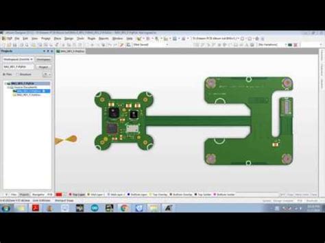
Creating the PCB Layout
Step 1: Generate a PCB from the Schematic
- Go to Design > Update PCB Document.
- Choose Create PCB from Schematic if prompted.
- Specify the board settings, such as size and layer stack.
Step 2: Place Components
- Arrange components on the PCB based on your design requirements.
- Consider factors like component size, placement, and routing constraints.
Step 3: Route the PCB
- Use the Interactive Routing tool to manually route traces between components.
- Adjust trace widths and clearances as needed.
- Use the Auto-Route feature for complex designs or to save time.
Step 4: Add Copper Pours and Planes
- Define copper pour regions for power and ground planes.
- Specify the net name and clearance settings for each pour.
- Use the Polygon Pour tool to fill the regions with copper.
Step 5: Perform Design Rule Checks (DRC)
- Configure the design rules based on your PCB manufacturer’s specifications.
- Run a Design Rule Check to identify and resolve any errors or violations.
Generating Manufacturing Files
Step 1: Create a Bill of Materials (BOM)
- Go to Reports > Bill of Materials.
- Customize the BOM template and output format.
- Generate the BOM and save it as a spreadsheet or text file.
Step 2: Generate Gerber Files
- Go to File > Fabrication Outputs > Gerber Files.
- Select the layers to include in the Gerber output.
- Specify the output directory and file format.
- Generate the Gerber files for PCB manufacturing.
Step 3: Generate Drill Files
- Go to File > Fabrication Outputs > NC Drill Files.
- Configure the drill file settings, such as tool sizes and units.
- Generate the drill files for PCB manufacturing.
Collaborating with Your Team
Altium Designer offers several collaboration features to streamline your PCB design process:
- Version Control: Integrate with version control systems like Git or SVN to manage design revisions and track changes.
- Altium 365: Use Altium’s cloud platform to share and collaborate on projects with your team in real time.
- MCAD Co-Design: Collaborate with mechanical designers using MCAD tools like SolidWorks or Inventor for seamless electro-mechanical integration.
Frequently Asked Questions (FAQ)
1. What is the difference between Altium Designer and other PCB design software?
Altium Designer is a comprehensive EDA software package that offers schematic capture, 3D PCB design, FPGA system design, and simulation tools in a single integrated environment. It provides advanced features and automation capabilities compared to many other PCB design software options.
2. Is Altium Designer suitable for beginners?
While Altium Designer is a powerful and feature-rich software, it may have a steeper learning curve compared to simpler PCB design tools. However, with the help of tutorials, documentation, and a supportive community, beginners can learn and master Altium Designer over time.
3. How much does Altium Designer cost?
Altium Designer is a premium software package, and its pricing varies based on the license type and duration. Visit the Altium website or contact their sales team for up-to-date pricing information and available licensing options.
4. Can I import designs from other PCB software into Altium Designer?
Yes, Altium Designer supports importing designs from various PCB File formats, including Eagle, KiCad, and ODB++. You can use the File > Import command to bring your existing designs into Altium Designer.
5. Where can I find additional resources and support for Altium Designer?
Altium provides extensive documentation, tutorial videos, and a knowledge base on their website. Additionally, there are active user forums, such as the Altium Designer Forum and EDABoard.com, where you can ask questions and interact with experienced designers. Altium also offers professional training courses and support services for users who need further assistance.
By following this step-by-step Altium Designer tutorial and exploring the software’s features and capabilities, you’ll be well on your way to designing professional-grade PCBs. Remember to refer to the official Altium documentation and resources for more detailed information and advanced topics. Happy designing!
No responses yet