Understanding Trace Impedance
Trace impedance is a critical factor in the design of high-speed printed circuit boards (PCBs). It refers to the opposition to the flow of alternating current (AC) in a trace, which is a conducting path on a PCB. Proper control of trace impedance is essential for maintaining signal integrity, minimizing reflections, and ensuring reliable communication between components.
Factors Affecting Trace Impedance
Several factors influence the impedance of a trace on a PCB:
-
Trace width: The width of the trace affects its impedance. Wider traces have lower impedance, while narrower traces have higher impedance.
-
Trace thickness: The thickness of the copper trace also impacts its impedance. Thicker traces have lower impedance compared to thinner traces.
-
Dielectric constant: The dielectric constant of the PCB material between the trace and the reference plane affects the trace impedance. Materials with higher dielectric constants result in lower impedance.
-
Height above ground plane: The distance between the trace and the reference plane (usually a ground plane) influences the trace impedance. Increasing the height above the ground plane leads to higher impedance.
-
Frequency: Trace impedance is frequency-dependent. At higher frequencies, the impedance of a trace may change due to factors such as skin effect and dielectric losses.
Calculating Trace Impedance
To ensure proper impedance matching and signal integrity, it is essential to calculate the trace impedance during the PCB design process. There are several methods and formulas used to calculate trace impedance, depending on the trace geometry and the PCB Stackup.
Microstrip Trace Impedance Formula
A microstrip is a trace on the outer layer of a PCB, with a reference plane (usually a ground plane) on the layer below. The impedance of a microstrip trace can be calculated using the following formula:
Z₀ = (87 / √(ɛᵣ + 1.41)) * ln(5.98 * h / (0.8 * w + t))
Where:
– Z₀ is the characteristic impedance of the microstrip trace in ohms (Ω)
– ɛᵣ is the relative dielectric constant of the PCB material
– h is the height of the trace above the reference plane in mils (thousandths of an inch)
– w is the width of the trace in mils
– t is the thickness of the trace in mils
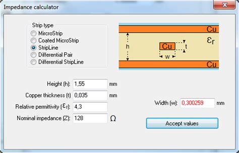
Stripline Trace Impedance Formula
A stripline is a trace embedded within the inner layers of a PCB, with reference planes (usually ground planes) above and below the trace. The impedance of a stripline trace can be calculated using the following formula:
Z₀ = (60 / √ɛᵣ) * ln((1.9 * (2*h + t)) / (0.8 * w + t))
Where:
– Z₀ is the characteristic impedance of the stripline trace in ohms (Ω)
– ɛᵣ is the relative dielectric constant of the PCB material
– h is the height of the trace above the reference plane in mils (thousandths of an inch)
– w is the width of the trace in mils
– t is the thickness of the trace in mils
Coplanar Waveguide Trace Impedance Formula
A coplanar waveguide (CPW) is a trace on the outer layer of a PCB, with ground planes on either side of the trace. The impedance of a CPW trace can be calculated using the following formula:
Z₀ = (30π / √ɛᵣ) * (K(k) / K'(k))
Where:
– Z₀ is the characteristic impedance of the CPW trace in ohms (Ω)
– ɛᵣ is the relative dielectric constant of the PCB material
– K(k) and K'(k) are complete elliptic integrals of the first kind
– k = w / (w + 2*s)
– w is the width of the trace in mils
– s is the gap between the trace and the ground planes in mils
Impedance Control in PCB Manufacturing
Achieving the desired trace impedance in a manufactured PCB requires careful control of the fabrication process. PCB manufacturers use various techniques to ensure that the actual trace impedance matches the designed impedance within acceptable tolerances.
Impedance Tolerance
The impedance tolerance specifies the allowable deviation of the actual trace impedance from the designed impedance. Common impedance tolerances are:
- ±10% for general-purpose designs
- ±5% for high-speed designs
- ±2% for very high-speed designs
Tighter impedance tolerances require more precise control of the PCB manufacturing process and may increase the cost of fabrication.
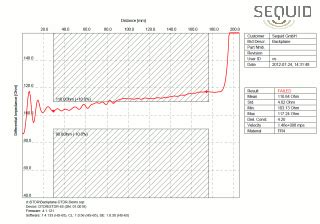
Impedance Testing
To verify that the manufactured PCB meets the specified impedance requirements, manufacturers perform impedance testing. There are two primary methods for impedance testing:
-
Time Domain Reflectometry (TDR): TDR involves sending a fast-rising pulse down the trace and measuring the reflections caused by impedance discontinuities. By analyzing the reflected waveform, the impedance profile of the trace can be determined.
-
Frequency Domain Reflectometry (FDR): FDR uses a vector network analyzer (VNA) to measure the S-parameters of the trace over a range of frequencies. The S-parameters can be used to calculate the characteristic impedance of the trace.
Impedance Control Techniques
PCB manufacturers employ various techniques to control the trace impedance during fabrication:
-
Trace width and spacing control: Precise control of the trace width and spacing is essential for maintaining the desired impedance. Manufacturers use high-resolution photolithography and etching processes to achieve accurate trace geometries.
-
Dielectric thickness control: The thickness of the dielectric material between the trace and the reference plane directly affects the trace impedance. Manufacturers use precise lamination and drilling techniques to maintain consistent dielectric thicknesses.
-
Copper thickness control: The thickness of the copper trace also influences its impedance. Manufacturers use controlled electroplating and etching processes to achieve the specified copper thickness.
-
Material selection: The choice of PCB materials, such as the dielectric substrate and copper foil, can impact the trace impedance. Manufacturers work with material suppliers to ensure consistent material properties and performance.

Impedance calculators and Tools
To simplify the process of calculating trace impedance and designing controlled impedance PCBs, several calculators and tools are available. These tools help engineers determine the appropriate trace geometries and stackup configurations to achieve the desired impedance.
Online Impedance Calculators
There are many online impedance calculators that provide quick and easy access to trace impedance calculations. Some popular online calculators include:
- EEWeb Impedance Calculator
- Microstrip Impedance Calculator
- Omnicalculator Transmission Line Impedance Calculator
These calculators typically require inputs such as the trace geometry, dielectric constant, and substrate thickness, and provide the resulting characteristic impedance.
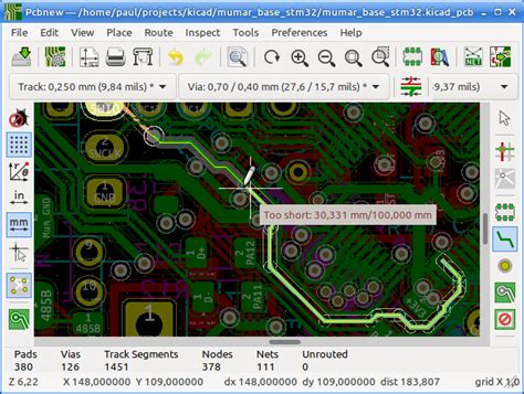
PCB Design Software
Most modern PCB design software packages include built-in tools for calculating and managing trace impedance. These tools allow designers to specify the desired impedance and automatically calculate the required trace geometries based on the PCB stackup and material properties. Some popular PCB design software with impedance control capabilities include:
- Altium Designer
- Cadence Allegro
- Mentor Graphics PADS
- KiCad
These tools often provide real-time feedback on the impedance of traces as they are being designed, helping engineers to optimize the PCB layout for controlled impedance.
Spreadsheet Calculators
For more flexibility and customization, some engineers prefer to use spreadsheet-based impedance calculators. These calculators allow users to input their specific design parameters and materials, and provide more control over the calculation process. Popular spreadsheet platforms for impedance calculations include:
- Microsoft Excel
- Google Sheets
- LibreOffice Calc
Spreadsheet calculators can be especially useful for comparing different design options and performing sensitivity analyses.
Trace Impedance Best Practices
To ensure successful controlled impedance PCB designs, consider the following best practices:
-
Choose the appropriate impedance: Select the target impedance based on the requirements of your application, such as the signaling standard, data rate, and rise time.
-
Consider the stackup: Design your PCB stackup to accommodate the desired impedance. This may involve adjusting the dielectric thickness, trace geometry, and reference plane spacing.
-
Use consistent geometry: Maintain consistent trace width and spacing throughout the length of the trace to avoid impedance discontinuities.
-
Minimize discontinuities: Avoid abrupt changes in trace geometry, such as sharp bends or vias, which can cause impedance discontinuities and reflections.
-
Provide adequate clearance: Ensure sufficient clearance between traces and other components to minimize crosstalk and maintain the desired impedance.
-
Simulate and validate: Use simulation tools to validate your controlled impedance design before manufacturing. Perform post-fabrication testing to verify that the actual impedance meets the specified requirements.
-
Collaborate with your manufacturer: Work closely with your PCB manufacturer to ensure that they can meet your impedance requirements and tolerances. Provide clear specifications and communicate any special considerations.
Frequently Asked Questions (FAQ)
- What is the difference between characteristic impedance and Differential Impedance?
-
Characteristic impedance refers to the impedance of a single trace with respect to a reference plane, such as a ground plane. Differential impedance, on the other hand, refers to the impedance between two traces in a differential pair, without considering the reference plane.
-
How does the dielectric constant affect trace impedance?
-
The dielectric constant of the PCB material between the trace and the reference plane affects the trace impedance. A higher dielectric constant results in lower impedance, while a lower dielectric constant leads to higher impedance. The dielectric constant is a property of the material and is frequency-dependent.
-
What is the typical impedance for a USB trace?
-
USB (Universal Serial Bus) traces are typically designed with a characteristic impedance of 90 ohms (±10%). This impedance is chosen to match the impedance of the USB cable and connectors, ensuring proper signal transmission and minimizing reflections.
-
Can I achieve controlled impedance on a two-layer PCB?
-
Yes, it is possible to achieve controlled impedance on a two-layer PCB. However, the design options are more limited compared to multi-layer PCBs. On a two-layer PCB, you can use microstrip traces with the appropriate width and spacing to achieve the desired impedance. The trade-off is that two-layer PCBs may have more limited routing space and may require larger trace geometries to achieve the same impedance as multi-layer designs.
-
What is the impact of trace impedance mismatch?
- Trace impedance mismatch can cause signal integrity issues, such as reflections, ringing, and signal distortion. When a signal encounters an impedance discontinuity, a portion of the signal energy is reflected back towards the source, leading to signal degradation and potential errors in communication. Proper impedance matching helps to minimize these issues and ensure reliable signal transmission.
Conclusion
Trace impedance is a critical consideration in the design of high-speed PCBs. Proper control of trace impedance is essential for maintaining signal integrity, minimizing reflections, and ensuring reliable communication between components. By understanding the factors that affect trace impedance and using appropriate calculators and formulas, designers can create controlled impedance PCBs that meet the requirements of their applications.
Achieving the desired trace impedance requires careful design, simulation, and collaboration with PCB manufacturers. By following best practices and using the right tools and techniques, engineers can successfully design and fabricate PCBs with controlled impedance, enabling the development of high-performance electronic systems.
No responses yet