Introduction to 3D PCBs
3D PCBs, or three-dimensional printed circuit boards, are a revolutionary technology that is transforming the electronics industry. Unlike traditional PCBs, which are flat and two-dimensional, 3D PCBs are designed and manufactured using advanced 3D printing techniques. This allows for the creation of complex, multi-layered structures that can incorporate electronic components, sensors, and other features directly into the PCB itself.
Benefits of 3D PCBs
- Increased design flexibility
- Improved performance and reliability
- Reduced size and weight
- Faster prototyping and production
- Lower costs for small-scale production
The Process of Creating a 3D PCB Video
Creating a video showcasing the process of designing and manufacturing a 3D PCB can be a valuable tool for educating others about this exciting technology. Here are the key steps involved in creating a 3D PCB video:
1. Planning and Scripting
Before you start filming, it’s important to have a clear plan and script for your video. This will help ensure that your content is well-organized, informative, and engaging. Consider the following factors when planning your video:
- Target audience
- Video length and format
- Key topics and talking points
- Visuals and graphics
- Call-to-action or desired outcome
2. Gathering Materials and Equipment
To create a high-quality 3D PCB video, you’ll need to have the right materials and equipment on hand. This may include:
- 3D printer and filament
- PCB design software
- Electronic components and tools
- Video camera and lighting equipment
- Editing software
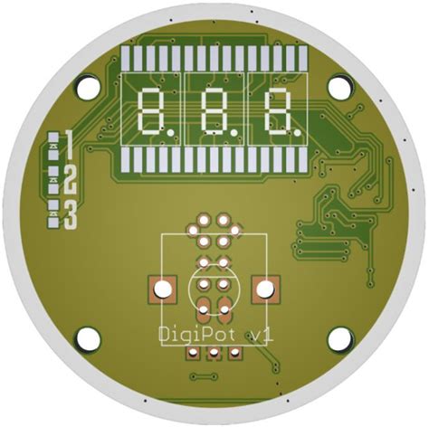
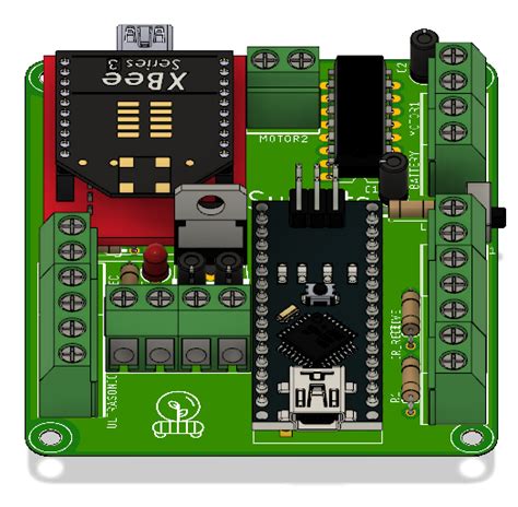
3. Designing the 3D PCB
The next step is to design your 3D PCB using specialized software. There are many different PCB design tools available, ranging from free, open-source options to professional-grade software suites. Some popular options include:
- KiCad
- Eagle
- Altium Designer
- Fusion 360
When designing your 3D PCB, consider factors such as:
- Component placement and orientation
- Signal integrity and EMI
- Thermal management
- Mechanical strength and durability
4. Printing the 3D PCB
Once your design is complete, it’s time to print your 3D PCB using a 3D printer. There are several different 3D printing technologies available, each with its own advantages and limitations. Some common options include:
- Fused Deposition Modeling (FDM)
- Stereolithography (SLA)
- Selective Laser Sintering (SLS)
- PolyJet
When printing your 3D PCB, be sure to follow the manufacturer’s guidelines for your specific printer and filament type. Pay close attention to factors such as:
- Print settings and parameters
- Support structures and removal
- Post-processing and finishing
5. Assembling and Testing the 3D PCB
After your 3D PCB has been printed, it’s time to assemble and test it. This may involve soldering components, programming microcontrollers, and conducting various electrical and functional tests. Be sure to document this process carefully for your video, as it can be a valuable learning experience for your viewers.
6. Editing and Publishing the Video
Finally, it’s time to edit your footage and publish your 3D PCB video. Use your editing software to create a polished, professional-looking final product that effectively conveys the key points you want to communicate. Consider adding elements such as:
- Titles and captions
- Background music and sound effects
- Transitions and animations
- Call-to-action or additional resources
Once your video is complete, publish it on your preferred platform (e.g., YouTube, Vimeo, your own website) and promote it through your social media channels and other relevant networks.
Advantages of 3D PCBs over Traditional PCBs
| Aspect | 3D PCBs | Traditional PCBs |
|---|---|---|
| Design Flexibility | High | Low |
| Component Integration | Excellent | Limited |
| Miniaturization | Significant | Moderate |
| Prototyping Speed | Fast | Slow |
| Small-Scale Production Costs | Low | High |
3D PCBs offer several key advantages over traditional PCBs, as summarized in the table above. These benefits make 3D PCBs an attractive option for a wide range of applications, from consumer electronics to aerospace and defense.
Design Flexibility
One of the primary advantages of 3D PCBs is their increased design flexibility. With traditional PCBs, designers are limited to a flat, two-dimensional layout. In contrast, 3D PCBs allow for complex, multi-layered structures that can incorporate electronic components, sensors, and other features directly into the PCB itself. This opens up new possibilities for innovative product designs and functionalities.
Component Integration
3D PCBs also offer superior component integration compared to traditional PCBs. By embedding components directly into the PCB structure, designers can create more compact, streamlined devices with fewer external connections and improved reliability. This can lead to better performance, reduced signal interference, and enhanced durability.
Miniaturization
Another key benefit of 3D PCBs is their potential for miniaturization. By leveraging the three-dimensional space available, designers can create smaller, more compact devices without sacrificing functionality or performance. This is particularly valuable in applications where size and weight are critical factors, such as wearable technology, medical devices, and aerospace systems.
Prototyping Speed
3D PCBs can also accelerate the prototyping process compared to traditional PCBs. With 3D printing technology, designers can quickly iterate on their designs and produce functional prototypes in a matter of hours or days, rather than weeks or months. This can help reduce development times, lower costs, and bring products to market faster.
Small-Scale Production Costs
Finally, 3D PCBs can offer significant cost savings for small-scale production runs. Traditional PCB manufacturing often requires high setup costs and minimum order quantities, making it expensive and impractical for low-volume production. In contrast, 3D printing allows for on-demand, small-batch production with minimal setup costs, making it an attractive option for startups, hobbyists, and niche markets.

Challenges and Limitations of 3D PCBs
While 3D PCBs offer many advantages, there are also several challenges and limitations to consider:
Material Properties
3D printed materials may not have the same electrical and mechanical properties as traditional PCB materials, such as FR-4. This can impact signal integrity, thermal management, and durability, requiring careful material selection and design optimization.
Resolution and Accuracy
The resolution and accuracy of 3D printers can vary widely depending on the specific technology and equipment used. This can affect the minimum feature sizes, layer thicknesses, and overall precision of the finished PCB, potentially limiting its performance and reliability.
Post-Processing
Many 3D printed PCBs require additional post-processing steps, such as support removal, sanding, and coating, to achieve the desired finish and functionality. These steps can add time and complexity to the manufacturing process, and may require specialized equipment or expertise.
Scalability
While 3D printing is well-suited for small-scale production and prototyping, it may not be as cost-effective or efficient for large-scale manufacturing compared to traditional PCB fabrication methods. This can limit the scalability of 3D PCBs for certain applications and markets.
Future Trends and Applications of 3D PCBs
Despite these challenges, the future of 3D PCBs looks bright, with many exciting trends and applications on the horizon:
Advanced Materials
Researchers and manufacturers are continually developing new materials for 3D printing, including conductive, insulating, and functional materials that can enhance the performance and capabilities of 3D PCBs. These advanced materials may enable new applications and design possibilities, such as embedded sensors, antennas, and energy storage devices.
Multi-Material Printing
Another promising trend is the development of multi-material 3D printing technologies, which can combine different materials with varying properties in a single print job. This could allow for the creation of highly integrated, multi-functional 3D PCBs with embedded components, interconnects, and other features, further pushing the boundaries of what is possible with this technology.
Artificial Intelligence and Generative Design
The integration of artificial intelligence (AI) and generative design tools into the 3D PCB design process could help optimize layouts, improve performance, and automate certain tasks. By leveraging AI algorithms and machine learning, designers could create more efficient, reliable, and innovative 3D PCBs in less time and with fewer resources.
Emerging Applications
As 3D PCB technology continues to advance, it is opening up new possibilities for a wide range of applications, including:
- Wearable technology and medical devices
- Aerospace and defense systems
- Automotive and transportation electronics
- Industrial automation and IoT
- Telecommunications and 5G networks
These emerging applications could drive further innovation and adoption of 3D PCBs in the coming years, transforming the way we design, manufacture, and use electronic devices.
Frequently Asked Questions (FAQ)
1. What software is needed to design a 3D PCB?
To design a 3D PCB, you’ll need specialized PCB design software that supports 3D modeling and layout. Some popular options include KiCad, Eagle, Altium Designer, and Fusion 360. These tools provide the necessary features and capabilities for creating complex, multi-layered 3D PCB designs.
2. What types of 3D printers are suitable for printing 3D PCBs?
Several 3D printing technologies can be used for creating 3D PCBs, including Fused Deposition Modeling (FDM), Stereolithography (SLA), Selective Laser Sintering (SLS), and PolyJet. The choice of printer will depend on factors such as the desired resolution, materials, and performance requirements of your specific application.
3. Can 3D printed PCBs be used for high-frequency applications?
While 3D printed PCBs can be used for high-frequency applications, designers must carefully consider factors such as material properties, feature sizes, and signal integrity to ensure optimal performance. Advanced materials and printing technologies, such as multi-material printing and conductive inks, may help address some of the challenges associated with high-frequency 3D PCBs.
4. How does the cost of 3D PCBs compare to traditional PCBs?
The cost of 3D PCBs compared to traditional PCBs can vary depending on factors such as production volume, design complexity, and material choices. For small-scale production and prototyping, 3D PCBs can offer significant cost savings due to lower setup costs and on-demand manufacturing capabilities. However, for large-scale production, traditional PCB manufacturing methods may still be more cost-effective.
5. What are some of the key challenges in adopting 3D PCB technology?
Some of the key challenges in adopting 3D PCB technology include limitations in material properties, resolution and accuracy of 3D printers, the need for post-processing steps, and scalability concerns for large-scale manufacturing. Additionally, designers and engineers may need to acquire new skills and knowledge to effectively leverage 3D PCB design and manufacturing processes. As the technology continues to evolve and mature, many of these challenges are likely to be addressed, making 3D PCBs an increasingly viable option for a wider range of applications.
Conclusion
3D PCBs represent a significant advancement in electronic design and manufacturing, offering numerous benefits over traditional PCBs. From increased design flexibility and component integration to faster prototyping and lower small-scale production costs, 3D PCBs have the potential to transform the way we create and use electronic devices.
By understanding the process of creating a 3D PCB video, exploring the advantages and limitations of this technology, and staying informed about future trends and applications, designers, engineers, and enthusiasts can effectively leverage 3D PCBs to drive innovation and push the boundaries of what is possible in the world of electronics.
As the technology continues to evolve and mature, it is likely that we will see even more exciting developments and applications emerge, further cementing the role of 3D PCBs in shaping the future of the electronics industry.
No responses yet