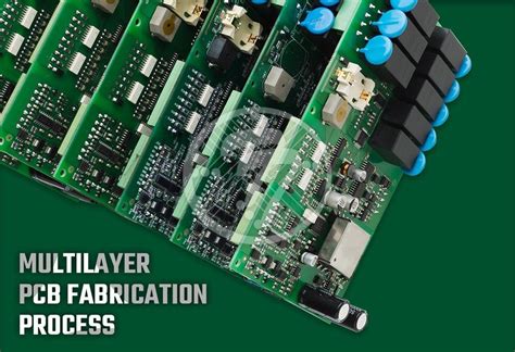
What is PCB Fabrication?
PCB fabrication is the process of creating a printed circuit board from a design file. The process involves multiple steps, including:
- PCB Design
- PCB Fabrication
- PCB Assembly
- PCB Testing
Each step in the process is critical for ensuring the quality and reliability of the final product.
PCB Design
The first step in PCB fabrication is designing the circuit board. This involves creating a schematic diagram of the circuit and laying out the components on the board. The design process typically involves the following steps:
-
Schematic Capture: The schematic diagram of the circuit is created using specialized software. The schematic shows the electrical connections between the components and provides a blueprint for the PCB layout.
-
Component Selection: The components required for the circuit are selected based on their electrical and mechanical properties. The selection process involves considering factors such as power rating, package size, and cost.
-
PCB Layout: The components are placed on the board, and the traces are routed to connect them. The layout process involves considering factors such as signal integrity, power distribution, and manufacturability.
-
Design Rule Check (DRC): The design is checked for compliance with the manufacturing guidelines and standards. The DRC ensures that the design can be manufactured reliably and cost-effectively.
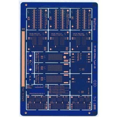
PCB Fabrication
Once the design is complete, the next step is to fabricate the PCB. The fabrication process involves the following steps:
-
Copper Clad Laminate: The process begins with a copper-clad laminate, which is a thin layer of copper bonded to a substrate material such as FR-4.
-
Drilling: Holes are drilled in the laminate to accommodate the components and vias. The drilling process is typically automated using computer numerical control (CNC) machines.
-
Patterning: The copper layer is patterned to create the traces and pads. This is typically done using a photolithographic process, where the copper is selectively etched away using a photoresist and etchant.
-
Plating: The holes and pads are plated with copper to improve the electrical and mechanical properties of the board. Additional layers of copper may be added to increase the current carrying capacity of the traces.
-
Solder Mask: A layer of solder mask is applied to the board to protect the copper traces and prevent short circuits. The solder mask also provides a surface for the silkscreen.
-
Silkscreen: The component designators and other markings are printed on the board using a silkscreen process.
-
Surface Finish: A surface finish such as HASL, ENIG, or OSP is applied to the board to protect the copper and improve solderability.
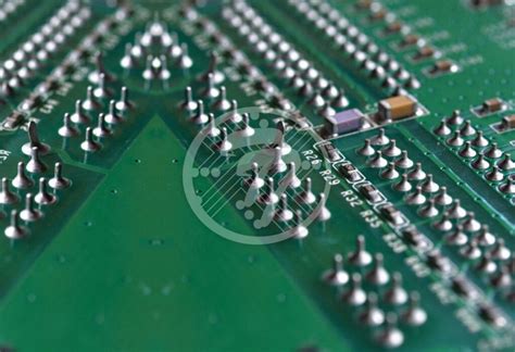
PCB Assembly
After the PCB is fabricated, the next step is to assemble the components onto the board. The assembly process involves the following steps:
-
Solder Paste Application: Solder paste is applied to the pads on the board using a stencil or screen printing process.
-
Component Placement: The components are placed on the board using automated pick-and-place machines or by hand.
-
Reflow Soldering: The board is heated in a reflow oven to melt the solder paste and form a permanent bond between the components and the board.
-
Inspection: The assembled board is inspected for defects such as bridging, tombstoning, or missing components.
PCB Testing
The final step in the PCB fabrication process is testing. The testing process involves verifying the functionality and reliability of the board. The following tests are commonly performed:
-
Continuity Test: The continuity of the traces and connections is tested using a multimeter or automated test equipment.
-
Functional Test: The board is powered up and tested for functionality using specialized test equipment or by connecting it to the intended system.
-
Environmental Test: The board may be subjected to environmental stresses such as temperature, humidity, or vibration to ensure reliability under real-world conditions.
Advanced PCB Fabrication Techniques
In addition to the basic PCB fabrication process, there are several advanced techniques that can be used to improve the performance and reliability of the board. Some of these techniques include:
High-Density Interconnect (HDI)
HDI is a PCB fabrication technique that involves using smaller vias and finer pitch components to increase the density of the board. HDI boards can be used to reduce the size and weight of the product while improving the signal integrity and power distribution.
Rigid-Flex PCBs
Rigid-flex PCBs are a type of PCB that combines rigid and flexible substrates to create a board that can be folded or bent. Rigid-flex PCBs are commonly used in applications where space is limited, or where the board needs to conform to a specific shape.
Embedded Components
Embedded components are a PCB fabrication technique where the components are embedded within the layers of the board. This technique can be used to reduce the size and weight of the board while improving the signal integrity and power distribution.
3D PCBs
3D PCBs are a type of PCB that incorporates multiple layers of circuitry in a three-dimensional structure. 3D PCBs can be used to create complex, high-density circuits that would be difficult or impossible to achieve with traditional 2D PCBs.
Choosing a PCB Fabrication Partner
Choosing the right PCB fabrication partner is critical for ensuring the success of your project. When selecting a PCB fabricator, consider the following factors:
-
Experience: Look for a fabricator with experience in manufacturing the type of PCB you require. Ask for references and samples of their work.
-
Capabilities: Ensure that the fabricator has the capabilities to manufacture your PCB to your specifications. This includes the ability to handle the required materials, copper weights, and surface finishes.
-
Quality: Look for a fabricator with a strong quality control process and a track record of producing high-quality boards. Ask about their testing and inspection procedures.
-
Lead Time: Consider the fabricator’s lead time and ensure that it aligns with your project timeline. Keep in mind that rush orders may incur additional costs.
-
Cost: Obtain quotes from multiple fabricators and compare the costs. Keep in mind that the lowest price may not always be the best value, particularly if the quality or lead time is compromised.

FAQ
- What is the difference between PCB fabrication and PCB assembly?
PCB fabrication is the process of creating the bare circuit board, while PCB assembly is the process of attaching the components to the board.
- What is the typical lead time for PCB fabrication?
The lead time for PCB fabrication can vary depending on the complexity of the board and the fabricator’s workload. Typical lead times range from 1-2 weeks for standard boards to 4-6 weeks for complex or high-volume orders.
- What is the minimum feature size that can be achieved with PCB fabrication?
The minimum feature size depends on the fabricator’s capabilities and the materials used. Typical minimum feature sizes range from 3-4 mils (0.003-0.004 inches) for standard boards to 1-2 mils for high-density boards.
- What is the difference between HASL and ENIG surface finishes?
HASL (Hot Air Solder Leveling) is a surface finish that involves dipping the board in molten solder to coat the copper. ENIG (Electroless Nickel Immersion Gold) is a surface finish that involves plating the copper with a layer of nickel and a thin layer of gold. ENIG provides better solderability and shelf life than HASL but is more expensive.
- Can I fabricate a PCB at home?
Yes, it is possible to fabricate simple PCBs at home using methods such as etching or milling. However, these methods are limited in terms of the complexity and precision that can be achieved. For high-quality, reliable PCBs, it is recommended to use a professional fabrication service.
Conclusion
PCB fabrication is a complex process that requires precision, attention to detail, and specialized equipment. Understanding the basics of PCB design, fabrication, assembly, and testing is essential for anyone involved in the development of electronic products. By following best practices and choosing the right fabrication partner, you can ensure the success of your PCB project and bring your electronic designs to life.
| Process | Description |
|---|---|
| PCB Design | Creating the schematic and layout of the circuit board |
| PCB Fabrication | Manufacturing the bare circuit board |
| PCB Assembly | Attaching the components to the board |
| PCB Testing | Verifying the functionality and reliability of the board |
No responses yet