Introduction to Controlled-Impedance PCBs
In the world of high-speed electronic design, signal integrity is paramount. As digital systems continue to push the boundaries of speed and bandwidth, the importance of maintaining clean, undistorted signals throughout the printed circuit board (PCB) becomes increasingly critical. This is where controlled-impedance PCBs come into play. By carefully designing the copper traces on the PCB to match a specific impedance value, engineers can minimize signal reflections, crosstalk, and other undesirable effects that can degrade signal quality and lead to system failures.
What is Impedance?
Before diving into the intricacies of controlled-impedance PCBs, it’s essential to understand the concept of impedance. In simple terms, impedance is a measure of the opposition that an electrical circuit presents to the flow of current when a voltage is applied. It is a complex quantity that takes into account both the resistance and reactance of the circuit. In the context of PCB design, impedance is typically expressed in ohms (Ω) and is determined by factors such as the geometry of the copper traces, the dielectric properties of the PCB substrate, and the frequency of the signals being transmitted.
Why is Impedance Matching Important?
When a signal travels along a copper trace on a PCB, it encounters a characteristic impedance that is determined by the properties of the trace and the surrounding environment. If the impedance of the trace matches the impedance of the source and the load, the signal will propagate smoothly without any reflections. However, if there is an impedance mismatch at any point along the signal path, a portion of the signal energy will be reflected back toward the source, causing distortions and potentially leading to signal integrity issues.
Impedance matching is particularly important in high-speed digital systems, where the rise and fall times of the signals are very short. In these cases, even small impedance mismatches can cause significant reflections, leading to problems such as:
- Signal distortion and loss of signal quality
- Increased electromagnetic interference (EMI) and crosstalk
- Reduced signal-to-noise ratio (SNR)
- Potential system failures due to false triggering or missed transitions
By ensuring that the impedance of the PCB traces matches the impedance of the source and load, designers can minimize these issues and maintain signal integrity throughout the system.
Designing Controlled-Impedance PCBs
Designing a controlled-impedance PCB requires careful consideration of several factors, including the geometry of the copper traces, the properties of the PCB substrate, and the characteristics of the signals being transmitted. The following sections will explore these factors in more detail and provide guidelines for designing PCBs with optimal signal integrity.
Trace Geometry
The geometry of the copper traces on a PCB plays a crucial role in determining their impedance. The key parameters that affect Trace Impedance are:
- Trace width: Wider traces have lower impedance, while narrower traces have higher impedance.
- Trace thickness: Thicker traces have lower impedance, while thinner traces have higher impedance.
- Trace spacing: The spacing between traces affects their mutual capacitance and inductance, which in turn affects their impedance.
To achieve a specific target impedance, designers must carefully choose the appropriate trace width, thickness, and spacing based on the properties of the PCB substrate and the frequency of the signals being transmitted. There are several industry-standard impedance values that are commonly used in PCB design, such as 50 Ω, 75 Ω, and 100 Ω.
| Impedance (Ω) | Typical Application |
|---|---|
| 50 | High-speed digital signals, RF circuits |
| 75 | Video signals, coaxial cables |
| 100 | Ethernet, LVDS (Low-Voltage Differential Signaling) |
To calculate the required trace geometry for a given target impedance, designers can use specialized software tools or refer to impedance calculation charts provided by PCB manufacturers. These tools take into account factors such as the dielectric constant and thickness of the PCB substrate, as well as the desired trace impedance and the operating frequency of the signals.
PCB Substrate Properties
The properties of the PCB substrate also play a significant role in determining the impedance of the copper traces. The two main substrate properties that affect impedance are:
- Dielectric constant (Dk): The dielectric constant is a measure of the substrate’s ability to store electrical energy. Higher Dk values result in lower trace impedance, while lower Dk values result in higher trace impedance.
- Dissipation factor (Df): The dissipation factor is a measure of the substrate’s ability to dissipate electrical energy as heat. Higher Df values result in higher losses and can affect signal integrity at high frequencies.
Common PCB substrate materials and their typical Dk and Df values are shown in the table below:
| Substrate Material | Dielectric Constant (Dk) | Dissipation Factor (Df) |
|---|---|---|
| FR-4 | 4.2 – 4.5 | 0.02 – 0.03 |
| Rogers RO4003C | 3.38 | 0.0027 |
| Isola IS410 | 3.9 – 4.1 | 0.015 – 0.017 |
| Teflon (PTFE) | 2.1 | 0.0002 |
When selecting a substrate material for a controlled-impedance PCB, designers must consider the trade-offs between the material’s electrical properties, cost, and manufacturing feasibility. In general, substrates with lower Dk and Df values are preferred for high-speed applications, as they result in higher trace impedance and lower losses. However, these materials may be more expensive and require specialized processing techniques compared to standard FR-4.
Signal Characteristics
The characteristics of the signals being transmitted on the PCB also influence the design of controlled-impedance traces. The two main signal characteristics to consider are:
- Frequency: The operating frequency of the signals determines the wavelength and the level of sensitivity to impedance mismatches. Higher frequencies require more stringent impedance control and may necessitate the use of advanced PCB materials and design techniques.
- Rise/fall times: The rise and fall times of the digital signals affect the bandwidth and the level of electromagnetic interference (EMI) generated by the traces. Faster rise and fall times require more careful impedance matching to minimize reflections and EMI.
To ensure optimal signal integrity, designers must choose the appropriate trace geometry and substrate material based on the frequency and rise/fall times of the signals being transmitted. In some cases, it may be necessary to use advanced techniques such as differential signaling or edge-coupled traces to further reduce EMI and improve signal quality.
Manufacturing Controlled-Impedance PCBs
Manufacturing controlled-impedance PCBs requires strict process control and specialized equipment to ensure that the finished board meets the specified impedance requirements. The following sections will discuss the key aspects of manufacturing controlled-impedance PCBs.
PCB Fabrication Process
The PCB fabrication process for controlled-impedance boards is similar to that of standard PCBs, with a few additional steps to ensure proper impedance control. The basic steps in the process are:
- Material selection: The appropriate substrate material is chosen based on the required electrical properties and the target impedance of the traces.
- Copper foil lamination: The substrate is laminated with copper foil on one or both sides, depending on the design requirements.
- Drilling and plating: Holes are drilled through the board and plated with copper to create vias and through-hole component pads.
- Patterning and etching: The copper foil is patterned and etched to create the desired trace geometry and spacing.
- Impedance Testing: The finished board is tested to verify that the actual trace impedance matches the specified target impedance within an acceptable tolerance.
Impedance Testing Methods
There are several methods for testing the impedance of PCB traces, each with its own advantages and limitations. The most common impedance testing methods are:
- Time Domain Reflectometry (TDR): TDR involves sending a fast rise time pulse down the trace and measuring the reflected signal to determine the impedance profile along the trace. TDR is widely used for impedance testing due to its ability to locate impedance discontinuities and provide detailed information about the trace geometry.
- Frequency Domain Reflectometry (FDR): FDR is similar to TDR but uses a swept frequency signal instead of a pulse. FDR is useful for measuring the impedance of traces over a wide frequency range and can provide information about the frequency-dependent behavior of the trace.
- Vector Network Analysis (VNA): VNA involves measuring the scattering parameters (S-parameters) of the trace using a network analyzer. VNA provides accurate measurements of the trace impedance, insertion loss, and return loss, but requires more complex and expensive equipment compared to TDR or FDR.
The choice of impedance testing method depends on factors such as the required accuracy, the available equipment, and the specific characteristics of the traces being tested. In general, TDR is the most commonly used method for production testing of controlled-impedance PCBs.
Impedance Tolerance and Control
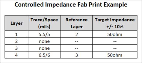
To ensure that the manufactured PCBs meet the specified impedance requirements, it is essential to establish appropriate impedance tolerances and control measures. Typical impedance tolerances for controlled-impedance PCBs are in the range of ±10% to ±15% of the target impedance value. For example, a 50 Ω trace with a ±10% tolerance would be acceptable if its actual impedance falls within the range of 45 Ω to 55 Ω.
To maintain impedance control during the manufacturing process, PCB fabricators employ several techniques, such as:
- Copper thickness control: Accurate control of the copper thickness is critical for achieving the desired trace impedance. PCB manufacturers use techniques such as controlled etching and plating to ensure consistent copper thickness across the board.
- Dielectric thickness control: The thickness of the PCB substrate directly affects the impedance of the traces. Manufacturers use precise lamination and pressing processes to maintain consistent dielectric thickness throughout the board.
- Trace width and spacing control: The width and spacing of the traces are critical for achieving the target impedance. PCB manufacturers use high-precision photolithography and etching processes to ensure accurate trace geometry and spacing.
By implementing these control measures and regularly testing the impedance of the manufactured PCBs, fabricators can ensure that the finished boards meet the specified impedance requirements and provide optimal signal integrity for the intended application.

Advantages of Controlled-Impedance PCBs
Controlled-impedance PCBs offer several key advantages over standard PCBs for high-speed and high-frequency applications. These advantages include:
- Improved signal integrity: By matching the impedance of the traces to the source and load impedances, controlled-impedance PCBs minimize signal reflections and distortions, resulting in cleaner and more reliable signals.
- Reduced EMI and crosstalk: Properly designed controlled-impedance traces reduce electromagnetic interference (EMI) and crosstalk between adjacent traces, which can be particularly problematic at high frequencies.
- Better power efficiency: Impedance-matched traces allow for more efficient transfer of power from the source to the load, reducing power losses and improving overall system efficiency.
- Increased system reliability: By minimizing signal integrity issues and reducing EMI, controlled-impedance PCBs contribute to increased system reliability and reduced risk of failures.
- Compatibility with advanced technologies: Controlled-impedance PCBs are essential for implementing advanced high-speed technologies such as DDR memory, PCI Express, and SerDes interfaces.
While controlled-impedance PCBs may have higher design and manufacturing costs compared to standard PCBs, the benefits they provide in terms of signal integrity, reliability, and performance make them a necessary investment for many high-speed and high-frequency applications.
FAQ
-
What is the main purpose of using controlled-impedance PCBs?
The main purpose of using controlled-impedance PCBs is to ensure optimal signal integrity and minimize signal distortions, reflections, and crosstalk in high-speed and high-frequency applications. -
What factors determine the impedance of a PCB trace?
The impedance of a PCB trace is determined by several factors, including the trace geometry (width, thickness, and spacing), the dielectric properties of the PCB substrate (dielectric constant and dissipation factor), and the frequency of the signals being transmitted. -
What are the typical impedance values used in controlled-impedance PCBs?
Common impedance values used in controlled-impedance PCBs include 50 Ω for high-speed digital signals and RF circuits, 75 Ω for video signals and coaxial cables, and 100 Ω for Ethernet and LVDS (Low-Voltage Differential Signaling) applications. -
What is the most common method for testing the impedance of PCB traces?
The most common method for testing the impedance of PCB traces is Time Domain Reflectometry (TDR), which involves sending a fast rise time pulse down the trace and measuring the reflected signal to determine the impedance profile along the trace. -
What are the key advantages of using controlled-impedance PCBs?
The key advantages of using controlled-impedance PCBs include improved signal integrity, reduced EMI and crosstalk, better power efficiency, increased system reliability, and compatibility with advanced high-speed technologies such as DDR memory, PCI Express, and SerDes interfaces.
Conclusion
Controlled-impedance PCBs are a critical component in modern high-speed and high-frequency electronic systems. By carefully designing the geometry and spacing of the copper traces and selecting appropriate substrate materials, engineers can ensure that the impedance of the traces matches the impedance of the source and load, minimizing signal integrity issues such as reflections, distortions, and crosstalk.
Designing and manufacturing controlled-impedance PCBs requires specialized knowledge, tools, and processes. PCB designers must consider factors such as trace geometry, substrate properties, and signal characteristics when calculating the required impedance and laying out the board. PCB manufacturers must employ strict process controls and use advanced techniques such as impedance testing and copper thickness control to ensure that the finished boards meet the specified impedance requirements.
While controlled-impedance PCBs may have higher costs compared to standard PCBs, the benefits they provide in terms of signal integrity, reliability, and performance make them an essential investment for many high-speed applications. As digital systems continue to push the boundaries of speed and bandwidth, the importance of controlled-impedance PCBs will only continue to grow, driving advances in PCB design and manufacturing technologies.
No responses yet