Introduction to PCB Design
Printed Circuit Board (PCB) design is a crucial aspect of modern electronics manufacturing. It involves the creation of a blueprint for the electrical connections and components that make up an electronic device. PCB design is a complex process that requires specialized knowledge and tools to ensure the final product meets the desired specifications and functions as intended.
The Importance of PCB Design
PCB design plays a vital role in the functionality, reliability, and cost-effectiveness of electronic devices. A well-designed PCB can:
- Ensure proper electrical connections and signal integrity
- Minimize electromagnetic interference (EMI) and crosstalk
- Optimize component placement for efficient use of space
- Facilitate efficient manufacturing processes
- Reduce overall production costs
The PCB Design Process
The PCB design process typically involves the following steps:
- Schematic Design: Create a schematic diagram that represents the electrical connections between components.
- Component Selection: Choose the appropriate components based on the device’s requirements and specifications.
- PCB Layout: Arrange the components and route the traces on the PCB using specialized software.
- Design Rule Check (DRC): Verify that the PCB layout meets the manufacturing and electrical requirements.
- Prototyping: Fabricate a prototype PCB to test and validate the design.
- Manufacturing: Mass-produce the PCB based on the final, validated design.
PCB Design Software
To create a PCB design, engineers and designers use specialized software tools. These tools allow them to create schematic diagrams, select components, and lay out the PCB. Some popular PCB design software packages include:
- Altium Designer
- OrCAD
- EAGLE
- KiCad
- Mentor Graphics PADS
| Software | Manufacturer | License Type | Key Features |
|---|---|---|---|
| Altium Designer | Altium | Commercial | Advanced routing, 3D visualization, simulation |
| OrCAD | Cadence | Commercial | Schematic capture, PCB layout, signal integrity analysis |
| EAGLE | Autodesk | Freemium | Schematic capture, PCB layout, extensive component libraries |
| KiCad | KiCad | Open-source | Schematic capture, PCB layout, 3D viewer, simulation |
| Mentor Graphics PADS | Mentor Graphics | Commercial | Schematic capture, PCB layout, constraint management |
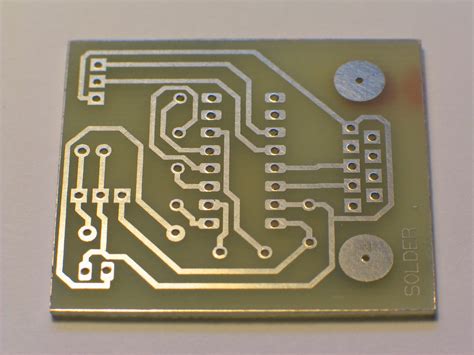
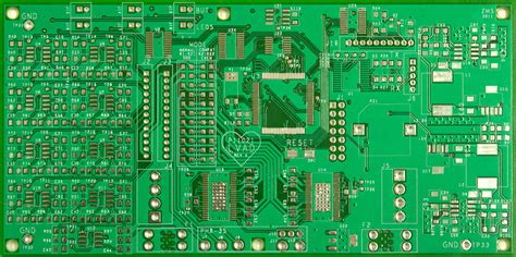
PCB Manufacturing Techniques
Once the PCB design is finalized and validated, it moves to the manufacturing stage. There are several techniques used in PCB manufacturing, each with its own advantages and limitations.
Through-Hole Technology (THT)
THT is the traditional method of PCB manufacturing, where component leads are inserted through drilled holes in the PCB and soldered on the opposite side. THT is known for its strong mechanical bonds and is suitable for larger components and high-power applications.
Surface Mount Technology (SMT)
SMT is a more modern approach to PCB manufacturing, where components are mounted directly onto the surface of the PCB without the need for drilled holes. SMT allows for smaller components, higher component density, and faster assembly processes.
Mixed Technology
Mixed technology PCBs combine both THT and SMT components on the same board. This approach is used when a device requires the benefits of both technologies, such as the use of large, high-power THT components alongside small, high-density SMT components.

PCB Materials
The choice of materials used in a PCB can significantly impact its performance, durability, and cost. The most common PCB materials include:
- FR-4: A glass-reinforced epoxy laminate, FR-4 is the most widely used PCB material due to its good electrical properties, mechanical strength, and cost-effectiveness.
- High-Frequency Materials: For applications requiring high-frequency operation, such as RF and microwave devices, specialized materials like Rogers RO4000 series or Teflon-based laminates are used to minimize signal loss and maintain signal integrity.
- Flexible Materials: Flexible PCBs are made using materials like polyimide or polyester to allow for bending and folding of the PCB, making them suitable for wearable electronics and space-constrained applications.
| Material | Dielectric Constant | Dissipation Factor | Key Characteristics |
|---|---|---|---|
| FR-4 | 4.2 – 4.6 | 0.02 – 0.03 | Good electrical properties, mechanical strength, cost-effective |
| Rogers RO4350B | 3.48 | 0.0037 | Low loss, stable dielectric constant, suitable for high-frequency |
| DuPont Pyralux AP | 3.4 | 0.002 | Flexible, high thermal stability, good chemical resistance |
PCB Assembly
After the PCB is manufactured, the components need to be assembled onto the board. The assembly process involves several steps, including:
- Solder Paste Application: Solder paste is applied to the pads on the PCB where components will be placed.
- Component Placement: Components are placed onto the PCB using automated pick-and-place machines or manual placement for THT components.
- Reflow Soldering: The PCB is heated in a reflow oven, melting the solder paste and creating a strong bond between the components and the PCB.
- Inspection: The assembled PCB is inspected for defects, such as misaligned components, solder bridges, or insufficient solder joints.
- Testing: The assembled PCB is tested to ensure it functions as intended and meets the required specifications.
PCB Design Considerations
When designing a PCB, engineers and designers must consider various factors to ensure the final product meets the desired performance, reliability, and cost targets. Some key considerations include:
Signal Integrity
Signal integrity refers to the ability of a PCB to maintain the quality and timing of electrical signals as they travel through the board. Factors that can affect signal integrity include:
- Trace width and spacing
- Trace Impedance
- Crosstalk between adjacent traces
- Electromagnetic interference (EMI)
Designers must carefully consider these factors and use techniques like proper trace routing, ground planes, and shielding to maintain signal integrity.
Thermal Management
Electronic components generate heat during operation, and excessive heat can lead to performance degradation or failure. PCB designers must consider thermal management techniques to ensure the board can effectively dissipate heat. Some common thermal management techniques include:
- Using thermal vias to transfer heat from components to the PCB’s ground plane
- Incorporating heatsinks or cooling fans
- Selecting components with appropriate power ratings and thermal characteristics
Manufacturing Constraints
PCB designers must also consider the limitations and requirements of the manufacturing process. Some key manufacturing constraints include:
- Minimum trace width and spacing
- Minimum drill hole size
- Clearance between components and the board edge
- Solder mask and silkscreen requirements
Designers must work closely with the manufacturing team to ensure the PCB design can be efficiently and reliably manufactured.
Frequently Asked Questions (FAQ)
1. What is the difference between a schematic and a PCB layout?
A schematic is a graphical representation of the electrical connections between components in a circuit. It shows how components are connected, but does not specify their physical location or the actual route of the connections. A PCB layout, on the other hand, is a physical representation of the circuit, showing the actual placement of components and the routing of traces on the PCB.
2. What is the purpose of a ground plane in a PCB?
A ground plane is a large area of copper on a PCB layer that is connected to the circuit’s ground potential. The purpose of a ground plane is to provide a low-impedance return path for electrical currents, which helps to reduce electromagnetic interference (EMI) and maintain signal integrity. Ground planes also help to distribute heat more evenly across the PCB.
3. What is the difference between through-hole and surface mount components?
Through-hole components have leads that are inserted through drilled holes in the PCB and soldered on the opposite side. Surface mount components, on the other hand, are mounted directly onto the surface of the PCB without the need for drilled holes. Surface mount components are generally smaller and allow for higher component density on the PCB, while through-hole components offer stronger mechanical bonds and are better suited for high-power applications.
4. What is the purpose of a solder mask on a PCB?
A solder mask is a protective layer applied to the copper traces on a PCB. It serves several purposes, including:
- Preventing solder bridges from forming between adjacent traces during the soldering process
- Protecting the copper traces from oxidation and corrosion
- Providing electrical insulation between components and traces
- Improving the PCB’s aesthetic appearance by covering the exposed copper
5. What is the role of a PCB designer in the product development process?
A PCB designer plays a crucial role in the product development process by creating the physical layout of the electronic circuit on the PCB. The designer works closely with electrical engineers, mechanical engineers, and the manufacturing team to ensure the PCB design meets the functional, performance, and manufacturing requirements of the product. Key responsibilities of a PCB designer include:
- Translating schematic diagrams into physical PCB layouts
- Selecting appropriate components and materials
- Optimizing component placement and trace routing for signal integrity and manufacturability
- Collaborating with the manufacturing team to ensure the PCB can be efficiently and reliably produced
- Continuously updating and revising the PCB design based on feedback from prototyping and testing
Conclusion
PCB design and manufacturing are essential aspects of modern electronics production. A well-designed and manufactured PCB is crucial for ensuring the functionality, reliability, and cost-effectiveness of electronic devices. By understanding the PCB design process, software tools, manufacturing techniques, materials, and assembly methods, engineers and designers can create high-quality PCBs that meet the ever-increasing demands of the electronics industry.
As technology continues to advance, PCB designers must stay up-to-date with the latest design techniques, materials, and manufacturing processes to create innovative and efficient electronic products. By considering factors such as signal integrity, thermal management, and manufacturing constraints, designers can optimize their PCB layouts for maximum performance and reliability.
Effective collaboration between PCB designers, electrical engineers, mechanical engineers, and manufacturing teams is essential for successful product development. By working together and leveraging their respective expertise, these professionals can bring innovative electronic products to market quickly and efficiently.
In conclusion, a deep understanding of PCB design and manufacturing is invaluable for anyone involved in the electronics industry. By mastering these concepts and staying current with the latest advancements, engineers and designers can create cutting-edge electronic products that drive technological progress and improve our daily lives.
No responses yet