Introduction to PCB Circuit Boards
A Printed Circuit Board (PCB) is a fundamental component in modern electronic devices. It serves as the backbone of an electronic system, providing mechanical support and electrical connectivity for various components such as resistors, capacitors, integrated circuits, and more. PCBs have revolutionized the electronics industry by enabling the miniaturization of devices, improving reliability, and reducing manufacturing costs.
In this comprehensive guide, we will delve into the world of PCB circuit boards, covering everything from the basics to advanced concepts. Whether you are an electronics enthusiast, a student, or a professional, this guide will provide you with valuable insights and knowledge about PCB design, fabrication, and assembly.
What is a PCB Circuit Board?
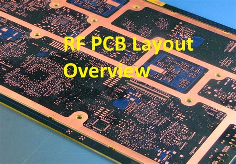
A PCB circuit board is a flat, insulating substrate made of materials like FR-4 (a composite of fiberglass and epoxy resin) or other laminate materials. The board consists of conductive tracks, pads, and other features etched from copper sheets laminated onto the substrate. These copper traces form the electrical connections between components mounted on the board.
PCBs come in various sizes, shapes, and types, depending on the specific application and requirements. They can be single-sided (with components and traces on one side), double-sided (with components and traces on both sides), or multi-layered (with multiple layers of copper traces sandwiched between insulating layers).
Advantages of PCB Circuit Boards
PCB circuit boards offer several advantages over traditional point-to-point wiring:
-
Compact Size: PCBs enable the miniaturization of electronic devices by allowing components to be closely packed together on a small board.
-
Reliability: The use of PCBs reduces the chances of loose connections and short circuits, resulting in improved reliability and durability of electronic devices.
-
Mass Production: PCBs are designed for automated assembly processes, enabling mass production of electronic devices at a lower cost.
-
Consistency: PCBs ensure consistent electrical characteristics and performance across multiple units of the same design.
-
Ease of Maintenance: PCBs make it easier to identify and replace faulty components, simplifying the maintenance and repair process.

PCB Design Process
The PCB design process involves several steps, from conceptualization to the final manufacturing of the board. Let’s take a closer look at each step:
1. Schematic Design
The first step in PCB design is creating a schematic diagram. A schematic is a graphical representation of the electronic circuit, showing the components and their interconnections. It serves as a blueprint for the PCB layout.
Schematic design involves selecting the appropriate components, defining their values and specifications, and creating the necessary connections between them. This step is typically done using Electronic Design Automation (EDA) software such as Altium Designer, Eagle, or KiCad.
2. Component Placement
Once the schematic is finalized, the next step is to place the components on the PCB layout. This process involves determining the optimal location for each component based on factors such as signal integrity, power distribution, thermal considerations, and mechanical constraints.
Component placement is a critical step as it directly impacts the overall performance and reliability of the PCB. It is important to consider factors such as component orientation, spacing, and thermal management to ensure proper functionality and manufacturability.
3. Routing
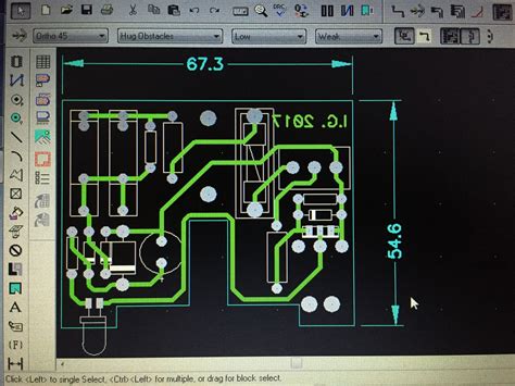
After the components are placed, the next step is to route the copper traces that connect the components together. Routing involves creating the conductive paths on the PCB that carry electrical signals between components.
Routing can be done manually or automatically using EDA software. The goal is to create efficient and reliable connections while minimizing signal interference, crosstalk, and electromagnetic compatibility (EMC) issues.
There are several factors to consider during routing, such as trace width, spacing, impedance matching, and signal integrity. Different routing strategies, such as through-hole routing, surface mount routing, and high-speed routing, may be employed depending on the specific requirements of the PCB.
4. Design Rule Check (DRC)
Before finalizing the PCB layout, it is essential to perform a Design Rule Check (DRC). DRC is an automated process that verifies the PCB layout against a set of predefined design rules and constraints.
The purpose of DRC is to identify any potential issues or violations in the PCB layout, such as short circuits, open circuits, insufficient clearances, or manufacturability problems. DRC helps ensure that the PCB design meets the required specifications and can be successfully manufactured.
5. Gerber File Generation
Once the PCB layout is finalized and passes the DRC, the next step is to generate Gerber files. Gerber files are industry-standard file formats used to communicate the PCB design information to the manufacturing process.
Gerber files contain the necessary data for each layer of the PCB, including copper layers, solder mask, silkscreen, and drill files. These files are used by PCB manufacturers to fabricate the physical board.

PCB Fabrication Process
The PCB fabrication process involves transforming the PCB design into a physical board. Let’s explore the key steps involved in PCB fabrication:
1. PCB material selection
The first step in PCB fabrication is selecting the appropriate PCB material based on the specific requirements of the application. The most commonly used PCB material is FR-4, which is a composite of fiberglass and epoxy resin.
Other PCB materials include:
– Polyimide: Used for high-temperature applications
– Ceramic: Used for high-frequency and high-power applications
– Aluminum: Used for heat dissipation and mechanical stability
The choice of PCB material depends on factors such as the operating environment, thermal requirements, dielectric properties, and cost.
2. Copper Cladding
The selected PCB material is then clad with a thin layer of copper on one or both sides. The copper cladding serves as the conductive layer for the PCB traces and pads.
The thickness of the copper cladding is specified in ounces per square foot (oz/ft²). Common copper thicknesses include 1 oz/ft² (35 µm), 2 oz/ft² (70 µm), and 3 oz/ft² (105 µm). Thicker copper layers are used for high-current applications or to improve thermal dissipation.
3. Drilling
Once the PCB material is clad with copper, the next step is to drill holes in the board. These holes serve various purposes, such as mounting through-hole components, creating vias for inter-layer connections, or providing mechanical support.
Drilling is typically done using computer numerical control (CNC) machines that operate with high precision and speed. The drill file generated during the PCB design process is used to guide the drilling process.
4. Patterning
After drilling, the next step is to create the desired copper pattern on the PCB. This is done through a process called photolithography.
The PCB is coated with a light-sensitive photoresist material and then exposed to UV light through a photomask that contains the copper pattern. The exposed areas of the photoresist become soluble and can be removed, leaving the desired copper pattern on the board.
5. Etching
The exposed copper areas are then etched away using a chemical etching process. The most common etching method is called subtractive etching, where the unwanted copper is removed, leaving only the desired copper traces and pads.
The etching process typically uses an acidic solution, such as ferric chloride or ammonium persulfate, to dissolve the copper. The PCB is then rinsed and cleaned to remove any remaining photoresist and etchant.
6. Soldermask Application
After etching, a soldermask layer is applied to the PCB. The soldermask is a protective coating that covers the copper traces, leaving only the exposed pads and areas where components will be soldered.
The soldermask serves several purposes, including:
– Protecting the copper traces from oxidation and corrosion
– Preventing solder bridges and short circuits during assembly
– Providing electrical insulation between adjacent traces
– Improving the aesthetics of the PCB
The soldermask is typically applied using a screen printing process and then cured using UV light or heat.
7. Silkscreen Printing
The final step in PCB fabrication is silkscreen printing. Silkscreen is a layer of text, symbols, or logos printed on the PCB for identification and assembly purposes.
Silkscreen printing is done using a screen printing process similar to the soldermask application. The silkscreen ink is typically white or yellow and is applied on top of the soldermask layer.
The silkscreen layer provides valuable information such as component designators, polarity markers, and test points, which aid in the assembly and troubleshooting of the PCB.

PCB Assembly Process
Once the PCB fabrication is complete, the next step is to assemble the components onto the board. The PCB assembly process involves several steps, including:
1. Solder Paste Application
Solder paste is a mixture of tiny solder particles suspended in a flux medium. It is applied to the PCB pads where surface mount components will be placed.
Solder paste application is typically done using a stencil printing process. A stencil with openings corresponding to the PCB pads is aligned with the board, and solder paste is spread across the stencil using a squeegee. The solder paste is deposited onto the pads through the openings in the stencil.
2. Component Placement
After solder paste application, the next step is to place the components onto the PCB. This process is called pick-and-place.
For surface mount components, automated pick-and-place machines are used to accurately place the components onto the solder paste-coated pads. These machines use vacuum nozzles to pick up the components from reels or trays and place them onto the PCB with high precision.
Through-hole components are typically inserted manually or using semi-automated insertion machines.
3. Reflow Soldering
Once the components are placed, the PCB undergoes a reflow soldering process. Reflow soldering involves heating the PCB and the components to a temperature that melts the solder paste, forming a permanent electrical and mechanical connection between the components and the PCB pads.
Reflow soldering is typically done in a reflow oven, which has a controlled temperature profile. The PCB passes through several temperature zones, including preheat, soak, reflow, and cooling zones. The solder paste melts and solidifies during this process, creating reliable solder joints.
4. Inspection and Testing
After the reflow soldering process, the assembled PCB undergoes inspection and testing to ensure its functionality and quality.
Visual inspection is performed to check for any visible defects, such as solder bridges, component misalignment, or missing components. Automated optical inspection (AOI) systems are often used for this purpose.
Electrical testing is conducted to verify the PCB’s functionality and performance. This can include in-circuit testing (ICT), boundary scan testing, or functional testing, depending on the complexity and requirements of the PCB.
5. Conformal Coating (Optional)
In some cases, a conformal coating may be applied to the assembled PCB for added protection against environmental factors such as moisture, dust, or chemicals.
Conformal coating is a thin, protective layer that covers the PCB and its components. It helps improve the PCB’s reliability and durability in harsh operating conditions.
Common conformal coating materials include acrylic, silicone, urethane, and parylene. The choice of coating material depends on the specific environmental requirements and the desired level of protection.
PCB Design Considerations
When designing a PCB, there are several key considerations to keep in mind to ensure optimal performance, reliability, and manufacturability. Let’s explore some of these considerations:
1. Signal Integrity
Signal integrity refers to the ability of a PCB to maintain the quality and integrity of the electrical signals passing through it. It is crucial to ensure that the signals reach their intended destinations without degradation, distortion, or interference.
To maintain signal integrity, designers need to consider factors such as:
– Trace width and spacing
– Impedance matching
– Crosstalk and electromagnetic interference (EMI)
– Grounding and shielding techniques
– Termination and routing strategies
Proper signal integrity design practices help minimize signal reflections, crosstalk, and other signal quality issues, resulting in a more reliable and robust PCB.
2. Power Integrity
Power integrity refers to the ability of a PCB to provide stable and clean power to all the components on the board. It involves managing the power distribution network (PDN) to ensure that each component receives the required voltage and current levels without excessive noise or voltage drops.
To achieve good power integrity, designers need to consider factors such as:
– Power plane design and placement
– Decoupling Capacitor Selection and placement
– Voltage regulation and filtering
– Current-carrying capacity of traces
– Thermal management
Proper power integrity design helps prevent issues such as voltage fluctuations, ground bounce, and electromagnetic interference (EMI), which can affect the overall performance and reliability of the PCB.
3. Thermal Management
Thermal management is an important consideration in PCB design, especially for high-power or high-density boards. It involves the effective dissipation of heat generated by components to prevent overheating and ensure reliable operation.
To manage thermal issues, designers can employ techniques such as:
– Proper component placement and spacing
– Use of thermal vias and heat sinks
– Selection of appropriate PCB materials with good thermal conductivity
– Airflow and cooling considerations
Effective thermal management helps prevent component failure, PCB Warpage, and other heat-related issues that can compromise the reliability and longevity of the PCB.
4. Electromagnetic Compatibility (EMC)
Electromagnetic compatibility (EMC) refers to the ability of a PCB to operate without causing or being affected by electromagnetic interference (EMI). EMI can disrupt the normal operation of electronic devices and cause signal integrity issues.
To ensure EMC, designers need to consider factors such as:
– Proper grounding and shielding techniques
– Minimizing loop areas and antenna effects
– Filtering and suppression of unwanted signals
– Compliance with EMC standards and regulations
Designing for EMC helps prevent interference issues, ensures the PCB’s compatibility with other electronic devices, and meets regulatory requirements.
5. Manufacturing Considerations
When designing a PCB, it is important to consider the manufacturability of the board. This involves designing the PCB in a way that facilitates efficient and cost-effective manufacturing processes.
Some key manufacturing considerations include:
– Adhering to design rules and constraints (DRC)
– Minimizing the number of layers and board size
– Using standard component packages and footprints
– Providing adequate spacing and clearances for assembly
– Specifying appropriate soldermask and silkscreen requirements
Designing for manufacturability helps reduce production costs, improves yield, and ensures the PCB can be reliably manufactured in volume.
Frequently Asked Questions (FAQ)
1. What is the difference between a PCB and a circuit board?
A PCB (Printed Circuit Board) is a specific type of circuit board that has conductive tracks, pads, and other features printed or etched onto a non-conductive substrate. In general, all PCBs are circuit boards, but not all circuit boards are PCBs. Circuit boards can also refer to other types of boards, such as breadboards or stripboards, which are used for prototyping or simple circuits.
2. What are the different types of PCBs?
There are several types of PCBs, including:
- Single-sided PCBs: Components and traces are on one side of the board.
- Double-sided PCBs: Components and traces are on both sides of the board.
- Multi-layer PCBs: Multiple layers of copper traces are sandwiched between insulating layers.
- Flexible PCBs: Made from flexible materials like polyimide, allowing the board to bend and conform to different shapes.
- Rigid-Flex PCBs: Combines rigid and flexible sections in a single board for added versatility.
3. What materials are used to make PCBs?
The most common material used for PCBs is FR-4, which is a composite of fiberglass and epoxy resin. Other materials include polyimide for high-temperature applications, ceramic for high-frequency and high-power applications, and aluminum for heat dissipation and mechanical stability.
4. What is the typical PCB design and manufacturing process?
The typical PCB design and manufacturing process involves the following steps:
- Schematic design: Creating a schematic diagram of the electronic circuit.
- Component placement: Placing components on the PCB layout.
- Routing: Creating the conductive paths (traces) that connect the components.
- Design Rule Check (DRC): Verifying the PCB layout against design rules and constraints.
- Gerber file generation: Generating files for manufacturing.
- PCB fabrication: Manufacturing the physical board, including material selection, copper cladding, drilling, patterning, etching, soldermask application, and silkscreen printing.
- PCB assembly: Assembling components onto the board, including solder paste application, component placement, reflow soldering, inspection, and testing.
5. What are some common PCB design software tools?
Some popular PCB design software tools include:
- Altium Designer
- Autodesk Eagle
- KiCad
- Cadence OrCAD
- Mentor Graphics PADS
These software tools provide schematic capture, PCB layout, routing, and simulation capabilities to aid in the design and development of PCBs.
Conclusion
PCB circuit boards are the backbone of modern electronics, providing a reliable and

No responses yet