Introduction to LGA Packaging
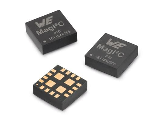
LGA is a type of surface-mount technology (SMT) package that uses a grid of flat contact pads on the bottom of the package to connect with the printed circuit board (PCB). Unlike Ball Grid Array (BGA) packages, LGA packages do not have balls or pins, making them more compact and cost-effective.
Key Features of LGA Packages
- Flat contact pads arranged in a grid pattern
- No balls or pins, resulting in a lower package height
- Excellent electrical and thermal performance
- High pin count capability
- Suitable for high-frequency applications
Advantages of LGA Packaging
LGA packaging offers several advantages over other packaging technologies, making it an attractive choice for various applications.
Improved Electrical Performance
The absence of balls or pins in LGA packages reduces the package’s overall inductance and capacitance, leading to improved electrical performance. This makes LGA packages suitable for high-frequency applications, such as radio frequency (RF) and microwave devices.
Enhanced Thermal Management
LGA packages have a lower thermal resistance compared to other packaging technologies, allowing for better heat dissipation. The flat contact pads provide a larger surface area for thermal transfer, enabling more efficient cooling of the IC.
Increased Reliability
LGA packages offer higher reliability compared to other SMT packages. The absence of fragile balls or pins reduces the risk of mechanical damage during handling and assembly. Additionally, the flat contact pads provide a more stable connection to the PCB, minimizing the chances of interconnect failures.
Space and Cost Savings
The compact nature of LGA packages allows for a smaller footprint on the PCB, saving valuable board space. This is particularly important in applications where miniaturization is critical, such as mobile devices and wearable electronics. Furthermore, the simplified manufacturing process and reduced material usage contribute to lower packaging costs.

LGA Package Variations
Several variations of LGA packages exist to cater to different application requirements.
Molded LGA (MLGA)
MLGA packages feature a plastic molding compound that encapsulates the IC and provides protection against environmental factors. This variation is commonly used in consumer electronics and automotive applications.
Cavity LGA (CLGA)
CLGA packages have a cavity in the substrate that houses the IC, allowing for better thermal management and enhanced electrical performance. This variation is often used in high-power applications, such as processors and field-programmable gate arrays (FPGAs).
Stacked LGA (SLGA)
SLGA packages enable the stacking of multiple ICs within a single package, increasing the package’s functionality and density. This variation is useful in applications that require high levels of integration, such as system-on-chip (SoC) designs.

Applications of LGA Packaging
LGA packaging finds applications in various industries and product categories.
Consumer Electronics
LGA packages are widely used in consumer electronics, such as smartphones, tablets, and wearable devices. The compact size and improved electrical performance of LGA packages make them ideal for these space-constrained and high-performance applications.
Automotive Electronics
The automotive industry increasingly relies on electronic systems for safety, infotainment, and powertrain control. LGA packages, with their enhanced reliability and thermal management capabilities, are well-suited for the demanding automotive environment.
Industrial and Medical Equipment
LGA packages are employed in industrial and medical equipment, where reliability and long-term performance are critical. The robust nature of LGA packages ensures stable operation in harsh environments and extends the equipment’s lifespan.
High-Performance Computing
High-performance computing applications, such as servers and data centers, benefit from the improved electrical performance and thermal management offered by LGA packages. The high pin count capability of LGA packages enables the integration of complex ICs with numerous interconnects.

Comparison with Other Packaging Technologies
To understand the advantages of LGA packaging, it is essential to compare it with other common packaging technologies.
LGA vs. BGA
BGA packages use solder balls to connect with the PCB, while LGA packages employ flat contact pads. LGA packages offer a lower package height, improved thermal management, and reduced manufacturing costs compared to BGA packages. However, BGA packages provide better self-alignment during assembly and are more suitable for applications with high pin counts.
LGA vs. QFN
Quad Flat No-lead (QFN) packages are another type of SMT package that shares some similarities with LGA packages. Both packages have a low profile and use perimeter leads for connection to the PCB. However, LGA packages offer a higher pin count capability and better thermal management compared to QFN packages.
LGA vs. PGA
Pin Grid Array (PGA) packages use an array of pins to connect with the PCB, while LGA packages use flat contact pads. LGA packages provide a lower profile, improved electrical performance, and better thermal management compared to PGA packages. Additionally, LGA packages are more suitable for surface mounting, while PGA packages are typically used in through-hole mounting applications.
Manufacturing and Assembly Considerations
When implementing LGA packaging in a product, several manufacturing and assembly considerations must be taken into account.
PCB Design Guidelines
Designing a PCB for LGA packages requires adherence to specific guidelines to ensure proper functionality and reliability. Key aspects include pad size and spacing, solder mask design, and via placement. Following the package manufacturer’s recommendations and industry standards is crucial for successful LGA package integration.
Assembly Process
The assembly process for LGA packages involves several steps, including solder paste printing, package placement, and reflow soldering. Accurate alignment and precise control of the reflow profile are essential to achieve reliable connections between the package and the PCB. Automated assembly equipment, such as pick-and-place machines and reflow ovens, is commonly used to ensure consistent and efficient assembly.
Inspection and Testing
Post-assembly inspection and testing are critical to verify the integrity of LGA package connections and overall product functionality. Visual inspection, automated optical inspection (AOI), and X-ray inspection are commonly employed techniques. Electrical testing, such as boundary scan and functional testing, helps identify any performance issues or defects.
Future Trends in LGA Packaging
As technology advances and demands for higher performance and miniaturization increase, LGA packaging is expected to evolve to meet these challenges.
Finer Pitch and Higher Pin Counts
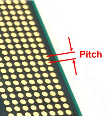
The trend towards finer pitch and higher pin counts in LGA packages will continue, enabling the integration of more complex and feature-rich ICs. This will require advancements in substrate materials, manufacturing processes, and assembly techniques to maintain reliability and performance.
3D Packaging
3D packaging, which involves stacking multiple ICs vertically, is gaining traction as a way to increase package density and functionality. LGA packages are well-suited for 3D packaging due to their low profile and good thermal management capabilities. Innovations in die stacking, through-silicon vias (TSVs), and interposer technologies will drive the adoption of 3D LGA packages.
Advanced Materials
The development of advanced materials, such as high-performance substrates and Thermal Interface materials (TIMs), will further enhance the electrical and thermal performance of LGA packages. These materials will enable LGA packages to meet the demanding requirements of emerging applications, such as 5G networks, artificial intelligence, and high-performance computing.
Frequently Asked Questions (FAQ)
-
Q: What is the main difference between LGA and BGA packages?
A: The main difference between LGA and BGA packages lies in the connection method. LGA packages use flat contact pads, while BGA packages use solder balls to connect with the PCB. LGA packages offer a lower profile and better thermal management, while BGA packages provide better self-alignment during assembly. -
Q: Can LGA packages be used for high-frequency applications?
A: Yes, LGA packages are well-suited for high-frequency applications due to their improved electrical performance. The absence of balls or pins reduces the package’s inductance and capacitance, making them ideal for RF and microwave devices. -
Q: How does the thermal management of LGA packages compare to other packaging technologies?
A: LGA packages offer better thermal management compared to other packaging technologies, such as BGA and QFN. The flat contact pads provide a larger surface area for thermal transfer, allowing for more efficient heat dissipation from the IC. -
Q: Are LGA packages suitable for automotive applications?
A: Yes, LGA packages are suitable for automotive applications due to their enhanced reliability and thermal management capabilities. The robust nature of LGA packages ensures stable operation in the demanding automotive environment, where temperature fluctuations and vibrations are common. -
Q: What are the key considerations when designing a PCB for LGA packages?
A: When designing a PCB for LGA packages, key considerations include pad size and spacing, solder mask design, and via placement. It is essential to follow the package manufacturer’s recommendations and industry standards to ensure proper functionality and reliability of the LGA package connection.
Conclusion
LGA packaging technology offers numerous advantages, including improved electrical performance, enhanced thermal management, increased reliability, and space and cost savings. These benefits make LGA packages an attractive choice for a wide range of applications, from consumer electronics to automotive and industrial systems.
As technology continues to advance, LGA packaging is expected to evolve, with trends towards finer pitch, higher pin counts, 3D packaging, and the use of advanced materials. By understanding the fundamentals of LGA packaging and its advantages, engineers and designers can make informed decisions when selecting the most suitable packaging technology for their products.
Embracing LGA packaging technology can help companies stay competitive in today’s rapidly evolving electronics landscape, enabling them to deliver high-performance, reliable, and cost-effective solutions to their customers.
| Packaging Technology | Key Features | Advantages | Disadvantages |
|---|---|---|---|
| LGA | – Flat contact pads – No balls or pins – Low profile |
– Improved electrical performance – Enhanced thermal management – Increased reliability – Space and cost savings |
– Requires precise PCB design and assembly – Limited self-alignment during assembly |
| BGA | – Solder balls for connection – Higher profile than LGA |
– Better self-alignment during assembly – Suitable for high pin count applications |
– Higher package height – Increased manufacturing costs – Less efficient thermal management |
| QFN | – Perimeter leads for connection – Low profile |
– Compact size – Cost-effective – Suitable for low pin count applications |
– Limited pin count capability – Less efficient thermal management compared to LGA |
| PGA | – Array of pins for connection – High profile |
– Suitable for through-hole mounting – Robust connection |
– Increased package height – Less efficient electrical and thermal performance compared to LGA – Not suitable for surface mounting |

No responses yet