What is Solder Mask?
Solder mask, also known as solder resist or solder stop, is a protective coating applied to the copper traces of a printed circuit board (PCB) to prevent accidental shorting and to protect the copper from oxidation. The solder mask material is typically a polymer-based ink that is applied to the PCB surface and then cured using heat or ultraviolet (UV) light.
The main functions of solder mask are:
- Insulation: Solder mask prevents accidental electrical shorts between adjacent copper traces or components.
- Protection: It protects the copper traces from oxidation, corrosion, and mechanical damage during the assembly process and throughout the life of the PCB.
- Aesthetics: Solder mask provides a professional appearance to the PCB and can be used to create text, logos, or other markings on the board surface.
Types of Solder Mask
There are two main types of solder mask materials:
-
Liquid Photoimageable Solder Mask (LPISM): This type of solder mask is applied as a liquid and then exposed to UV light through a photomask to create the desired pattern. LPISM is the most common type of solder mask used in the PCB industry due to its ease of application, high resolution, and excellent adhesion properties.
-
Dry Film Solder Mask (DFSM): This type of solder mask is a solid film that is laminated onto the PCB surface using heat and pressure. DFSM is less common than LPISM but is still used in some applications where high mechanical strength or chemical resistance is required.
Solder Mask Colors
Solder mask is available in a variety of colors, with green being the most common. Other popular colors include blue, red, yellow, black, and white. The choice of color is often a matter of personal preference or branding, but there are some practical considerations as well. For example, white solder mask is often used for LED lighting applications because it reflects light better than other colors.
Solder Mask Material Properties
The performance of a solder mask is determined by its material properties. Some of the key properties to consider when selecting a solder mask material include:
-
Adhesion: The solder mask must adhere well to the copper traces and the PCB substrate to provide effective protection and insulation.
-
Dielectric strength: The solder mask must have a high dielectric strength to prevent electrical breakdown and shorting between traces.
-
Thermal resistance: The solder mask must be able to withstand the high temperatures used during the soldering process without degrading or delaminating.
-
Chemical resistance: The solder mask must be resistant to the chemicals used in the PCB manufacturing process, such as cleaning agents and fluxes.
-
Flexibility: The solder mask must be flexible enough to accommodate any bending or flexing of the PCB during assembly or use.
-
Resolution: The solder mask must be able to resolve fine features and openings, such as small vias and component pads.
Solder Mask Material Comparison
The following table compares the properties of some common solder mask materials:
| Material | Adhesion | Dielectric Strength | Thermal Resistance | Chemical Resistance | Flexibility | Resolution |
|---|---|---|---|---|---|---|
| LPISM | Excellent | High | Good | Good | Good | Excellent |
| DFSM | Good | High | Excellent | Excellent | Fair | Good |
| Epoxy | Excellent | High | Excellent | Excellent | Fair | Fair |
| Acrylic | Good | Moderate | Good | Fair | Excellent | Good |
Solder Mask Application Process
The solder mask application process varies depending on the type of material being used, but the general steps are as follows:
-
Cleaning: The PCB surface is cleaned to remove any contaminants or residues that could affect the adhesion of the solder mask.
-
Application: The solder mask material is applied to the PCB surface using a screen printing, spraying, or lamination process.
-
Imaging: For LPISM, the solder mask is exposed to UV light through a photomask to create the desired pattern. For DFSM, the film is laminated onto the PCB surface using heat and pressure.
-
Developing: For LPISM, the unexposed areas of the solder mask are removed using a chemical developer, leaving only the desired pattern on the PCB surface.
-
Curing: The solder mask is cured using heat or UV light to crosslink the polymer and improve its mechanical and chemical properties.
-
Inspection: The PCB is inspected for any defects or imperfections in the solder mask, such as pinholes, bubbles, or misalignment.
Solder Mask Design Considerations
When designing a PCB with solder mask, there are several factors to consider to ensure optimal performance and manufacturability:
-
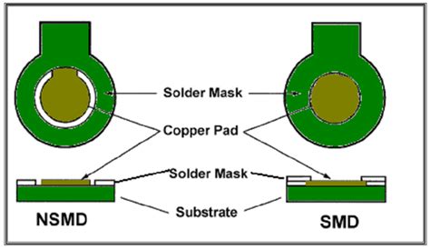
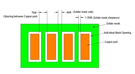
Clearance: The solder mask must have sufficient clearance around component pads and vias to allow for proper soldering and to prevent bridging or shorting.
-
Thickness: The solder mask thickness should be sufficient to provide adequate insulation and protection, but not so thick that it interferes with component placement or soldering.
-
Apertures: The solder mask apertures (openings) must be properly sized and positioned to allow for accurate component placement and soldering.
-
Marking: Any text, logos, or other markings on the solder mask must be properly designed and positioned to ensure legibility and durability.

Solder Mask Defects and Troubleshooting
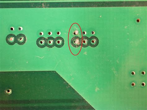
Despite careful design and application, solder mask defects can still occur. Some common solder mask defects include:
-
Pinholes: Small holes or voids in the solder mask that can allow moisture or contaminants to reach the copper traces.
-
Bubbles: Air bubbles trapped in the solder mask during application that can reduce its insulation and protection properties.
-
Misalignment: Misalignment of the solder mask relative to the copper traces or component pads, which can cause shorting or soldering issues.
-
Delamination: Separation of the solder mask from the PCB surface due to poor adhesion or thermal stress.
To troubleshoot solder mask defects, the following steps can be taken:
-
Inspection: Visually inspect the PCB for any visible defects or anomalies in the solder mask.
-
Testing: Perform electrical testing to check for shorts, opens, or other issues that could be caused by solder mask defects.
-
Analysis: Use microscopy or other analytical techniques to identify the root cause of the defect, such as contamination, improper curing, or material incompatibility.
-
Correction: Depending on the nature and severity of the defect, the PCB may need to be reworked, repaired, or scrapped.
FAQ
-
What is the difference between solder mask and conformal coating?
Solder mask is a permanent coating applied to the copper traces of a PCB to prevent shorting and provide protection. Conformal coating is a temporary coating applied to the entire PCB assembly to provide additional protection against moisture, dust, and other environmental factors. -
Can solder mask be removed?
Solder mask is designed to be a permanent coating and is difficult to remove once cured. However, it can be removed using specialized chemicals or abrasive methods, such as sanding or grinding, but this can also damage the underlying copper traces. -
What is the typical thickness of solder mask?
The typical thickness of solder mask ranges from 0.5 to 2.0 mils (0.0127 to 0.0508 mm), depending on the application and material used. Thicker solder mask provides better insulation and protection but can also interfere with component placement and soldering. -
Can solder mask be applied to flexible PCBs?
Yes, solder mask can be applied to flexible PCBs, but the material and application process must be chosen carefully to ensure adequate flexibility and adhesion. Some specialized solder mask materials, such as polyimide or silicone-based inks, are specifically designed for Flexible PCB Applications. -
How does solder mask affect PCB impedance?
Solder mask can affect PCB impedance by changing the dielectric constant of the PCB surface. This can cause impedance mismatches and signal integrity issues, particularly at high frequencies. To minimize this effect, the solder mask material and thickness must be carefully chosen and controlled, and the PCB Design must take the solder mask into account.
Conclusion
Solder mask is a critical component of PCB manufacturing that provides essential insulation, protection, and aesthetics to the finished board. The choice of solder mask material and application process depends on the specific requirements of the PCB, such as the operating environment, component density, and performance needs.
By understanding the properties and limitations of different solder mask materials, designers and manufacturers can optimize the PCB design and manufacturing process to ensure reliable and cost-effective production. Proper design, application, and inspection of the solder mask are essential to preventing defects and ensuring the long-term reliability of the PCB.
As PCB technology continues to advance, new solder mask materials and processes are being developed to meet the ever-increasing demands for performance, reliability, and sustainability. By staying up-to-date with the latest developments in solder mask technology, PCB professionals can ensure that their products remain competitive and meet the needs of their customers.
No responses yet