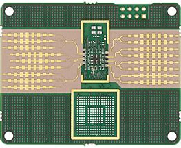
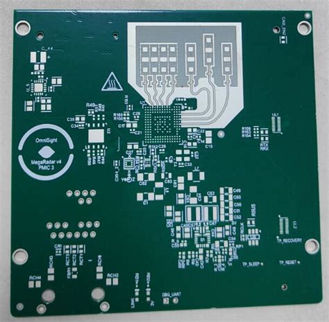
Introduction to Radar PCB
A radar PCB, or printed circuit board, is a specialized electronic circuit designed to facilitate the operation of radar systems. Radar, which stands for Radio Detection and Ranging, is a technology that uses radio waves to determine the distance, angle, and velocity of objects. Radar PCBs play a crucial role in the functionality and performance of radar systems, enabling accurate detection and automation in various applications.
Key Components of a Radar PCB
A radar PCB consists of several essential components that work together to generate, transmit, and receive radio frequency (RF) signals. These components include:
- RF Transmitter: Generates and amplifies the RF signal to be transmitted by the antenna.
- RF Receiver: Detects and processes the returned RF signal from the target object.
- Antenna: Transmits the RF signal and receives the reflected signal from the target object.
- Signal Processing Unit: Analyzes the received signal to determine the distance, angle, and velocity of the target object.
- Power Supply: Provides stable and regulated power to all components on the radar PCB.
Advantages of Using Radar PCBs
Radar PCBs offer several advantages over traditional radar systems, including:
- Compact Size: Radar PCBs are designed to be compact and lightweight, making them suitable for integration into various devices and systems.
- Cost-Effective: The use of PCB technology reduces the overall cost of radar systems, making them more accessible for a wide range of applications.
- Improved Reliability: Radar PCBs are designed to withstand harsh environmental conditions and provide reliable performance over an extended period.
- Customization: Radar PCBs can be customized to meet specific application requirements, such as frequency range, power output, and signal processing capabilities.
Radar PCB Design Considerations
Designing a radar PCB requires careful consideration of several factors to ensure optimal performance and reliability. Some of the key design considerations include:
Frequency Selection
The choice of operating frequency is crucial in radar PCB design. The frequency determines the range, resolution, and penetration capabilities of the radar system. Common frequency bands used in radar applications include:
| Frequency Band | Frequency Range |
|---|---|
| L-band | 1-2 GHz |
| S-band | 2-4 GHz |
| C-band | 4-8 GHz |
| X-band | 8-12 GHz |
| Ku-band | 12-18 GHz |
| K-band | 18-27 GHz |
| Ka-band | 27-40 GHz |
| V-band | 40-75 GHz |
| W-band | 75-110 GHz |
Signal Integrity
Maintaining signal integrity is essential in radar PCB design. The high-frequency nature of radar signals makes them susceptible to noise, interference, and signal distortion. To ensure signal integrity, designers must consider:
- Impedance Matching: Ensuring proper impedance matching between the transmitter, receiver, and antenna to minimize signal reflections and losses.
- Grounding and Shielding: Implementing proper grounding and shielding techniques to reduce electromagnetic interference (EMI) and cross-talk between components.
- Trace Routing: Optimizing trace routing to minimize Signal Delays, reflections, and coupling between traces.
Power Management
Efficient power management is crucial for the reliable operation of radar PCBs. Designers must ensure that the power supply provides stable and regulated power to all components on the board. Power management considerations include:
- Voltage Regulation: Implementing voltage regulators to provide stable and accurate voltage levels to different components on the radar PCB.
- Decoupling Capacitors: Using decoupling capacitors to suppress noise and ripple on power supply lines, ensuring clean and stable power delivery to components.
- Thermal Management: Designing the PCB layout to facilitate proper heat dissipation, preventing overheating of components and ensuring reliable operation.
Radar PCB Manufacturing Process
The manufacturing process of radar PCBs involves several steps to ensure high quality and reliability. The key stages in the manufacturing process include:
PCB Fabrication
- PCB Design: The radar PCB design is created using electronic design automation (EDA) software, generating the necessary Gerber files for manufacturing.
- Material Selection: The appropriate PCB substrate material, such as FR-4 or Rogers, is selected based on the frequency range and performance requirements of the radar system.
- Copper Cladding: The substrate is coated with a thin layer of copper on one or both sides, depending on the design requirements.
- Photolithography: The PCB design pattern is transferred onto the copper-clad substrate using photolithography, which involves applying a photoresist layer, exposing it to UV light through a photomask, and developing the pattern.
- Etching: The exposed copper areas are chemically etched away, leaving the desired conductive traces on the substrate.
- Drilling: Holes are drilled through the PCB for component mounting and via connections.
- Surface Finishing: The PCB undergoes surface finishing, such as HASL (Hot Air Solder Leveling) or ENIG (Electroless Nickel Immersion Gold), to protect the copper traces and improve solderability.
Component Assembly
- Solder Paste Application: Solder paste is applied to the PCB pads using a stencil or screen printing process.
- Component Placement: The electronic components, such as ICs, resistors, and capacitors, are placed on the PCB using automated pick-and-place machines or manual placement for smaller batches.
- Reflow Soldering: The PCB with the placed components undergoes a reflow soldering process, where the board is heated in a controlled manner to melt the solder paste and create strong electrical and mechanical connections between the components and the PCB.
- Inspection and Testing: The assembled radar PCB undergoes visual inspection and automated optical inspection (AOI) to detect any assembly defects. Electrical testing is performed to ensure proper functionality and performance of the radar system.

Radar PCB Testing and Validation
To ensure the reliability and performance of radar PCBs, rigorous testing and validation processes are implemented. Some of the key testing methods include:
Functional Testing
Functional testing involves verifying the basic operation of the radar PCB, including:
- Power-On Test: Ensuring that the radar PCB powers on correctly and all components receive the required voltage levels.
- Transmitter Test: Verifying that the RF transmitter generates the expected output power and frequency.
- Receiver Test: Checking the receiver’s ability to detect and process the returned RF signal accurately.
- Signal Processing Test: Validating the functionality of the signal processing unit in determining the distance, angle, and velocity of the target object.
Environmental Testing
Environmental testing is performed to ensure that the radar PCB can withstand the operating conditions it will be exposed to. Common environmental tests include:
- Temperature Cycling: Subjecting the radar PCB to repeated cycles of high and low temperatures to verify its performance and reliability under extreme temperature conditions.
- Humidity Testing: Exposing the radar PCB to high humidity levels to assess its resistance to moisture and potential corrosion.
- Vibration and Shock Testing: Evaluating the radar PCB’s ability to withstand mechanical stresses and vibrations encountered during operation.
Electromagnetic Compatibility (EMC) Testing
EMC testing is crucial to ensure that the radar PCB operates without causing or being affected by electromagnetic interference. EMC tests include:
- Radiated Emissions Testing: Measuring the electromagnetic emissions generated by the radar PCB to ensure compliance with regulatory standards.
- Radiated Immunity Testing: Assessing the radar PCB’s ability to function correctly in the presence of external electromagnetic fields.
- Conducted Emissions and Susceptibility Testing: Evaluating the radar PCB’s impact on and susceptibility to electromagnetic disturbances conducted through power and signal lines.
Applications of Radar PCBs
Radar PCBs find applications in a wide range of industries and sectors, including:
Automotive Industry
Radar PCBs are extensively used in advanced driver assistance systems (ADAS) and autonomous vehicles for:
- Collision Avoidance: Detecting obstacles and other vehicles to prevent collisions.
- Adaptive Cruise Control: Maintaining a safe distance from the vehicle ahead by automatically adjusting the speed.
- Blind Spot Detection: Monitoring the vehicle’s blind spots and alerting the driver of potential hazards.
- Parking Assistance: Aiding drivers in parking maneuvers by detecting nearby objects and providing guidance.
Aerospace and Defense
Radar PCBs play a crucial role in aerospace and defense applications, such as:
- Air Traffic Control: Monitoring and managing aircraft movements in the airspace.
- Military Surveillance: Detecting and tracking enemy targets, including aircraft, missiles, and ground vehicles.
- Weather Monitoring: Providing real-time weather data for aviation and meteorological purposes.
- Satellite Communication: Enabling long-range communication and data transmission between ground stations and satellites.
Industrial Automation
Radar PCBs are used in various industrial automation applications, including:
- Level Measurement: Monitoring the level of liquids or solids in tanks and silos.
- Proximity Sensing: Detecting the presence or absence of objects in manufacturing and packaging processes.
- Conveyor Control: Tracking and controlling the movement of items on conveyor belts.
- Robotics: Enabling robots to navigate, avoid obstacles, and interact with their environment.
Healthcare
Radar PCBs find applications in healthcare, such as:
- Remote Patient Monitoring: Tracking vital signs and movements of patients remotely.
- Fall Detection: Detecting falls in elderly or vulnerable individuals and alerting caregivers.
- Respiratory Monitoring: Monitoring breathing patterns and detecting abnormalities.
- Gesture Recognition: Enabling touchless control of medical devices and systems.
Frequently Asked Questions (FAQ)
1. What is the difference between a radar PCB and a conventional PCB?
A radar PCB is specifically designed to operate at high frequencies and handle RF signals, unlike conventional PCBs that are used for lower frequency applications. Radar PCBs require specialized materials, design techniques, and manufacturing processes to ensure optimal performance and reliability in radar systems.
2. What are the key challenges in designing a radar PCB?
Some of the key challenges in designing a radar PCB include maintaining signal integrity at high frequencies, ensuring proper impedance matching, minimizing electromagnetic interference, and managing power consumption and heat dissipation. Designers must also consider the specific requirements of the radar application, such as frequency range, power output, and signal processing capabilities.
3. How do I select the appropriate frequency band for my radar PCB?
The selection of the frequency band depends on the specific requirements of the radar application, such as the desired range, resolution, and penetration capabilities. Lower frequencies, such as L-band and S-band, offer longer range but lower resolution, while higher frequencies, such as X-band and K-band, provide higher resolution but shorter range. Designers must also consider the availability of components and the regulatory requirements for the chosen frequency band.
4. What are the common materials used for radar PCB substrates?
Common materials used for radar PCB substrates include FR-4, which is a low-cost and widely available material suitable for lower frequency applications, and high-frequency laminates such as Rogers RO4000 series, which offer superior dielectric properties and low loss at higher frequencies. The choice of substrate material depends on the frequency range, performance requirements, and cost constraints of the radar application.
5. How can I ensure the reliability and longevity of my radar PCB?
To ensure the reliability and longevity of a radar PCB, designers must follow best practices in PCB design, such as proper grounding and shielding, impedance matching, and power management. The manufacturing process should also adhere to strict quality control standards, including visual and automated optical inspection, and rigorous testing and validation procedures. Additionally, the radar PCB should be designed to withstand the environmental conditions it will be exposed to, such as temperature extremes, humidity, and mechanical stresses.
Conclusion
Radar PCBs are essential components in the development of advanced radar systems for detection and automation. By understanding the key design considerations, manufacturing processes, and testing methodologies, engineers can create high-performance and reliable radar PCBs for a wide range of applications, including automotive, aerospace, industrial automation, and healthcare.
As technology continues to evolve, the demand for compact, cost-effective, and high-performance radar solutions will continue to grow. Radar PCBs will play a crucial role in enabling the development of next-generation radar systems that offer improved accuracy, resolution, and functionality.
By staying up-to-date with the latest advancements in radar PCB technology and best practices in design and manufacturing, engineers can create innovative solutions that drive progress in various industries and contribute to the development of safer, more efficient, and more intelligent systems.
No responses yet