Introduction to RAYPCB Standard Stackup
RAYPCB is a leading manufacturer of high-quality printed circuit boards (PCBs) that cater to various industries, including consumer electronics, automotive, aerospace, and medical devices. One of the key factors that set RAYPCB apart from its competitors is its adherence to a standard stackup for Multilayer PCBs. This standard stackup ensures consistent performance, reliability, and manufacturability across all their products.
What is a PCB Stackup?
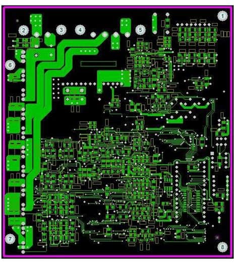
A PCB stackup refers to the arrangement of copper layers, insulating materials, and other components that make up a printed circuit board. It defines the number of layers, their thickness, and the materials used in the construction of the PCB. The stackup plays a crucial role in determining the electrical, mechanical, and thermal properties of the PCB.
Why is a Standard Stackup Important?
Having a standard stackup offers several advantages, including:
-
Consistency: By using a standard stackup, RAYPCB ensures that all their PCBs have consistent electrical and mechanical properties, regardless of the specific application or customer requirements.
-
Reliability: A well-designed standard stackup takes into account factors such as signal integrity, power distribution, and thermal management, resulting in more reliable PCBs.
-
Manufacturability: Standardizing the stackup allows RAYPCB to optimize their manufacturing processes, reducing the likelihood of errors and improving overall efficiency.
-
Cost-effectiveness: By using a standard stackup, RAYPCB can minimize the need for custom materials and processes, which helps to reduce costs and lead times for their customers.
RAYPCB Standard Stackup Components
The RAYPCB standard stackup for multilayer PCBs consists of several key components, each playing a specific role in the overall performance and reliability of the board.
Copper Layers
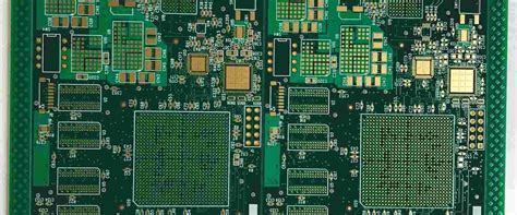
Copper layers are the conductive pathways that carry electrical signals and power throughout the PCB. The number of copper layers in a PCB can vary depending on the complexity of the design and the specific requirements of the application. RAYPCB’s standard stackup includes options for 4, 6, 8, 10, and 12 copper layers.
| Number of Layers | Typical Applications |
|---|---|
| 4 | Simple digital designs, low-speed analog circuits |
| 6 | Mixed-signal designs, moderate-speed digital circuits |
| 8 | Complex digital designs, high-speed interfaces |
| 10 | High-density designs, advanced mixed-signal circuits |
| 12 | Ultra-high-density designs, high-performance systems |
Insulating Materials
Insulating materials, also known as dielectrics, are used to separate and support the copper layers in the PCB stackup. RAYPCB’s standard stackup uses a combination of FR-4 laminate and prepreg materials.
-
FR-4 Laminate: FR-4 is a glass-reinforced epoxy laminate that forms the core of the PCB. It provides mechanical stability and electrical insulation between the copper layers.
-
Prepreg: Prepreg is a partially cured B-stage epoxy resin that is used to bond the copper layers and FR-4 laminates together. It also provides additional insulation and helps to control the thickness of the PCB.
Solder Mask and Silkscreen
Solder mask and silkscreen are applied to the outer layers of the PCB to protect the copper traces and provide labeling and identification of components.
-
Solder Mask: Solder mask is a polymer coating that covers the copper traces on the outer layers of the PCB, leaving only the exposed pads for component soldering. It protects the traces from oxidation and prevents solder bridges during the assembly process.
-
Silkscreen: Silkscreen is a printed layer that provides text, logos, and other identifying marks on the PCB surface. It helps with component placement and identification during assembly and troubleshooting.
RAYPCB Standard stackup design Guidelines
To ensure optimal performance and manufacturability, RAYPCB follows a set of design guidelines when implementing their standard stackup.
Signal Integrity
Signal integrity is crucial for maintaining the quality and reliability of electrical signals in the PCB. RAYPCB’s standard stackup addresses signal integrity concerns through the following practices:
-
Controlled Impedance: By carefully selecting the dielectric materials and copper trace geometries, RAYPCB can control the impedance of the signal traces, minimizing reflections and ensuring proper termination.
-
Differential pairs: For high-speed differential signals, RAYPCB’s standard stackup includes tightly coupled differential pairs with well-controlled spacing and impedance.
-
Ground Planes: The standard stackup incorporates dedicated ground planes to provide a low-impedance return path for signals and to minimize crosstalk between adjacent traces.
Power Distribution
Proper power distribution is essential for maintaining voltage stability and minimizing noise in the PCB. RAYPCB’s standard stackup addresses power distribution through the following techniques:
-
Power Planes: Dedicated power planes are used to distribute power evenly across the PCB, minimizing voltage drop and providing a low-impedance supply to the components.
-
Decoupling Capacitors: The standard stackup includes provisions for placing decoupling capacitors close to the power pins of active components, helping to reduce high-frequency noise and maintain voltage stability.
Thermal Management
Managing heat dissipation is critical for ensuring the long-term reliability and performance of the PCB. RAYPCB’s standard stackup incorporates several thermal management strategies:
-
Copper Thickness: The standard stackup specifies appropriate copper thicknesses for each layer, balancing electrical performance with the ability to dissipate heat.
-
Thermal Vias: The use of thermal vias helps to transfer heat from hot components to the inner layers and ultimately to the PCB’s heat sinks or cooling solutions.

RAYPCB Standard Stackup Manufacturing Process
RAYPCB’s standard stackup is manufactured using a well-controlled and optimized process that ensures consistent quality and reliability.
Material Selection
RAYPCB carefully selects the materials used in their standard stackup, including the FR-4 laminate, prepreg, copper foil, solder mask, and silkscreen ink. These materials are chosen based on their electrical, mechanical, and thermal properties, as well as their compatibility with the manufacturing process.
Lamination
The PCB stackup is assembled by alternating layers of FR-4 laminate, prepreg, and copper foil. The layers are aligned and pressed together under controlled temperature and pressure conditions to form a solid, bonded structure.
Drilling and Plating
After lamination, the PCB panel is drilled to create the necessary holes for vias, component leads, and mounting. The holes are then plated with copper to establish electrical connections between layers and to protect the exposed surfaces.
Patterning and Etching
The copper layers are patterned using a photolithographic process, which involves applying a light-sensitive resist, exposing it through a patterned mask, and developing the resist to reveal the desired copper traces. The unwanted copper is then removed using an etching process, leaving only the desired traces and pads.
Solder Mask and Silkscreen Application
Once the copper patterning is complete, the solder mask is applied to the outer layers of the PCB and cured using UV light. The silkscreen layer is then printed onto the solder mask using a screen-printing process.
Final Finishing and Inspection
The PCB panel undergoes a final surface finish, such as HASL (Hot Air Solder Leveling), ENIG (Electroless Nickel Immersion Gold), or OSP (Organic Solderability Preservative), to protect the exposed copper pads and improve solderability. The finished PCBs are then inspected for quality and conformance to specifications before being shipped to the customer.
Frequently Asked Questions (FAQ)
-
Q: What is the maximum number of layers supported by RAYPCB’s standard stackup?
A: RAYPCB’s standard stackup supports up to 12 copper layers for ultra-high-density designs and high-performance systems. -
Q: Can RAYPCB accommodate custom stackup requirements?
A: While RAYPCB strongly recommends using their standard stackup for optimal performance and manufacturability, they can work with customers to accommodate custom stackup requirements when necessary. -
Q: What is the typical lead time for PCBs using RAYPCB’s standard stackup?
A: Lead times can vary depending on the specific design and order quantity, but RAYPCB’s standardized processes and materials help to minimize lead times compared to custom stackups. -
Q: How does RAYPCB ensure the quality and reliability of their standard stackup?
A: RAYPCB follows strict design guidelines and manufacturing processes, uses carefully selected materials, and conducts thorough inspections to ensure the quality and reliability of their PCBs. -
Q: Can RAYPCB’s standard stackup be used for both prototype and production quantities?
A: Yes, RAYPCB’s standard stackup is suitable for both prototype and production quantities, ensuring consistent performance and manufacturability throughout the product lifecycle.
Conclusion
RAYPCB’s standard stackup for multilayer PCBs is a testament to their commitment to quality, reliability, and customer satisfaction. By adhering to a well-designed and carefully manufactured standard stackup, RAYPCB can offer their customers consistent performance, reduced lead times, and cost-effective solutions for a wide range of applications.
The standard stackup incorporates best practices for signal integrity, power distribution, and thermal management, ensuring that the resulting PCBs meet the demands of today’s complex electronic systems. Through the use of high-quality materials, well-controlled manufacturing processes, and rigorous inspection procedures, RAYPCB delivers PCBs that customers can rely on for their most challenging projects.
By choosing RAYPCB and their standard stackup for multilayer PCBs, customers can benefit from the company’s expertise, experience, and dedication to excellence in the PCB industry.
No responses yet