Introduction to PCB Fabrication
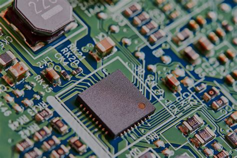
Printed Circuit Boards (PCBs) are the backbone of modern electronics. They provide a reliable and efficient way to connect electronic components in a compact and organized manner. PCB fabrication is a complex process that involves several steps, including design, etching, drilling, and finishing. One of the techniques used in PCB fabrication is called “mouse bites,” which is a method of creating perforations along the edges of a PCB panel to allow for easy separation of individual boards.
In this article, we will delve into the world of mouse bites PCB fabrication, exploring its benefits, applications, and the process involved in creating these unique PCBs.
What are Mouse Bites in PCB Fabrication?
Mouse bites, also known as nibble holes or break-away tabs, are small, circular perforations that are strategically placed along the edges of a PCB panel. These perforations are typically arranged in a linear pattern, resembling the bite marks of a mouse, hence the name “mouse bites.”
The primary purpose of mouse bites is to allow for easy separation of individual PCBs from a larger panel. Instead of using traditional methods like routing or scoring, which can be time-consuming and may cause damage to the boards, mouse bites provide a clean and efficient way to separate the PCBs.
Benefits of Using Mouse Bites in PCB Fabrication
-
Easy Separation: Mouse bites allow for quick and easy separation of individual PCBs from a larger panel, reducing the time and effort required in the fabrication process.
-
Minimized Damage: Compared to other separation methods, such as routing or scoring, mouse bites minimize the risk of damage to the PCBs during the separation process.
-
Improved Efficiency: By using mouse bites, PCB manufacturers can optimize their production process, reducing waste and increasing overall efficiency.
-
Cost-Effective: Mouse bites PCB fabrication is a cost-effective solution, as it eliminates the need for additional tooling or machinery for PCB separation.

Applications of Mouse Bites PCB
Mouse bites PCBs find applications in various industries and sectors, including:
-
Consumer Electronics: Mouse bites are commonly used in the production of consumer electronic devices, such as smartphones, tablets, and wearables, where compact and efficient PCB designs are crucial.
-
Automotive Industry: In the automotive sector, mouse bites PCBs are used in the fabrication of electronic control units (ECUs), sensors, and other electronic components.
-
Medical Devices: Mouse bites PCBs are utilized in the production of medical devices, such as patient monitors, diagnostic equipment, and wearable health devices.
-
Industrial Automation: In industrial automation, mouse bites PCBs are employed in the fabrication of sensors, controllers, and communication modules.

The Mouse Bites PCB Fabrication Process
The mouse bites PCB fabrication process involves several steps, each contributing to the creation of high-quality PCBs with easy-to-separate perforations.
Step 1: PCB Design
The first step in the mouse bites PCB fabrication process is the design phase. Using specialized PCB design software, engineers create the layout of the PCB, including the placement of components, traces, and the desired locations for the mouse bites.
During the design phase, considerations such as the size and spacing of the mouse bites, as well as their proximity to other features on the PCB, are taken into account to ensure optimal performance and manufacturability.
Step 2: PCB Panelization
Once the PCB design is finalized, the next step is panelization. In this process, multiple individual PCB designs are arranged on a larger panel, maximizing the utilization of the available space and minimizing waste.
The panelization process also involves the placement of the mouse bites along the edges of the panel, ensuring that each individual PCB can be easily separated after fabrication.
Step 3: Drilling and Etching
After panelization, the PCB panel undergoes drilling and etching processes. Holes are drilled through the panel at the designated locations for the mouse bites, as well as for other components and vias.
Next, the panel is subjected to an etching process, where the unwanted copper is removed from the surface of the board, leaving behind the desired traces and pads.
Step 4: Solder Mask Application
Once the drilling and etching processes are complete, a solder mask is applied to the PCB panel. The solder mask is a protective layer that covers the copper traces, leaving only the exposed pads and areas where components will be soldered.
The solder mask also helps to prevent short circuits and provides insulation between the copper traces.
Step 5: Silkscreen Printing
After the solder mask application, the next step is silkscreen printing. In this process, text, logos, and other markings are printed onto the surface of the PCB panel using a silkscreen printing technique.
These markings provide important information, such as component designators, polarity indicators, and other relevant details for assembly and troubleshooting.
Step 6: Surface Finish
To enhance the solderability and protect the exposed copper pads, a surface finish is applied to the PCB panel. Common surface finishes include Hot Air Solder Leveling (HASL), Immersion Silver, Immersion Tin, and Electroless Nickel Immersion Gold (ENIG).
The choice of surface finish depends on factors such as the intended application, environmental conditions, and the desired level of durability.
Step 7: Separation and Inspection
The final step in the mouse bites PCB fabrication process is the separation of individual PCBs from the panel. This is where the mouse bites come into play, allowing for easy and clean separation of the boards.
After separation, each individual PCB undergoes a thorough inspection to ensure that it meets the required quality standards. This inspection may include visual checks, electrical testing, and other quality control measures.

Advantages of Mouse Bites over Other Separation Methods
Mouse bites offer several advantages over other PCB separation methods, such as routing or scoring:
-
Cleaner Edges: Mouse bites result in cleaner and smoother edges compared to routing or scoring, reducing the risk of damage to the PCBs during separation.
-
Faster Separation: With mouse bites, the separation process is much faster, as the perforations allow for easy breaking of the panel into individual PCBs.
-
Reduced Stress: Mouse bites minimize the stress on the PCBs during separation, reducing the likelihood of cracking or other damage.
-
Improved Consistency: Mouse bites provide a more consistent and controlled separation process, ensuring that each PCB is separated with the same level of accuracy and quality.
Designing for Mouse Bites PCB Fabrication
When designing PCBs for mouse bites fabrication, several factors should be considered to ensure optimal results:
-
Bite Size and Spacing: The size and spacing of the mouse bites should be carefully chosen based on the thickness and material of the PCB, as well as the desired level of ease in separation.
-
Placement: Mouse bites should be placed strategically along the edges of the PCB, taking into account the location of other components, traces, and features.
-
Clearance: Adequate clearance should be maintained between the mouse bites and other features on the PCB to prevent any interference or damage during the fabrication process.
-
Panelization: When panelizing PCBs for mouse bites fabrication, it is essential to consider the overall layout and arrangement of the boards to maximize efficiency and minimize waste.
Frequently Asked Questions (FAQ)
-
What are mouse bites in PCB fabrication?
Mouse bites are small, circular perforations placed along the edges of a PCB panel to allow for easy separation of individual PCBs. -
What are the benefits of using mouse bites in PCB fabrication?
The benefits of using mouse bites include easy separation of PCBs, minimized damage, improved efficiency, and cost-effectiveness. -
What industries commonly use mouse bites PCBs?
Mouse bites PCBs are commonly used in industries such as consumer electronics, automotive, medical devices, and industrial automation. -
How do mouse bites compare to other PCB separation methods?
Mouse bites offer advantages over other separation methods, such as cleaner edges, faster separation, reduced stress, and improved consistency. -
What factors should be considered when designing for mouse bites PCB fabrication?
When designing for mouse bites PCB fabrication, factors such as bite size and spacing, placement, clearance, and panelization should be carefully considered to ensure optimal results.
Conclusion
Mouse bites PCB fabrication is a valuable technique in the production of printed circuit boards, offering numerous benefits, including easy separation, minimized damage, improved efficiency, and cost-effectiveness. By understanding the mouse bites fabrication process and considering key design factors, PCB manufacturers can create high-quality boards that meet the demands of various industries and applications.
As the electronics industry continues to evolve and innovate, mouse bites PCB fabrication remains an essential tool in the PCB manufacturer’s arsenal, enabling the production of compact, reliable, and efficiently designed circuit boards.
No responses yet