Introduction to PCB incoming inspection
The Printed Circuit Board (PCB) incoming inspection process is a crucial step in ensuring the quality and reliability of PCBs used in electronic devices. This process involves a series of checks and tests performed on PCBs received from suppliers to verify that they meet the required specifications and standards. The primary goal of PCB incoming inspection is to identify and prevent defective or non-conforming boards from entering the production line, thereby reducing the risk of product failures and customer complaints.
Importance of PCB Incoming Inspection
PCB incoming inspection is essential for several reasons:
- Quality assurance: By thoroughly inspecting incoming PCBs, manufacturers can ensure that only high-quality boards are used in their products.
- Cost reduction: Identifying defects early in the production process helps avoid the costs associated with rework, repairs, and product recalls.
- Reputation management: Delivering products with reliable and well-functioning PCBs helps maintain a positive brand reputation and customer satisfaction.
PCB Incoming Inspection Process Steps
The PCB incoming inspection process typically consists of several steps, each designed to assess different aspects of the PCBs. These steps may vary depending on the specific requirements of the manufacturer and the complexity of the PCBs being inspected.
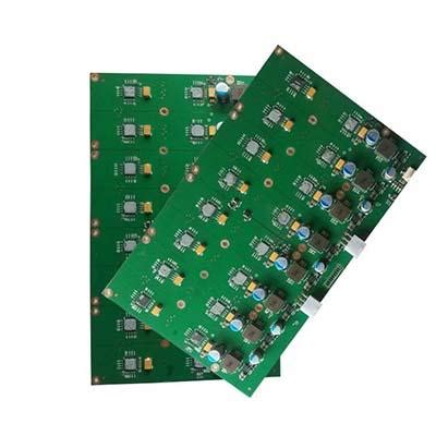
1. Visual Inspection
The first step in the PCB incoming inspection process is a visual examination of the boards. This inspection is performed to identify any obvious defects or irregularities that can be detected with the naked eye. Some of the aspects checked during visual inspection include:
- Board dimensions and thickness
- Solder mask and silkscreen quality
- Drilled holes and vias
- Surface finish uniformity
- Absence of scratches, dents, or contamination
Visual inspection is often performed using magnifying lenses or microscopes to ensure that even minor defects are detected.
2. Automated Optical Inspection (AOI)
Automated Optical Inspection (AOI) is a computer-based imaging system that uses cameras and image processing software to detect defects on PCBs. AOI systems can identify a wide range of defects, including:
- Solder bridging or shorts
- Missing or misaligned components
- Incorrect component polarity
- Insufficient or excessive solder
- Copper trace defects
AOI systems provide fast and accurate inspection results, making them an essential tool in the PCB incoming inspection process.
3. X-Ray Inspection
X-ray inspection is used to detect defects that are not visible on the surface of the PCB, such as:
- Solder joint quality (e.g., voids, insufficient solder)
- Proper placement of Ball Grid Array (BGA) components
- Internal delamination or cracks
X-ray inspection systems use high-resolution images generated by X-rays to create detailed cross-sectional views of the PCB and its components.
4. Electrical Testing
Electrical testing is performed to verify that the PCB functions as intended and meets the specified electrical requirements. Some common electrical tests include:
- Continuity testing: Verifies that the connections between components and traces are intact and have the correct resistance.
- Insulation testing: Checks for any short circuits or leakage between conductors.
- Functional testing: Ensures that the PCB performs its intended functions under various operating conditions.
Electrical testing can be performed using specialized equipment such as flying probe testers or in-circuit testers (ICT).
5. Solderability Testing
Solderability testing is conducted to assess the ease and reliability of soldering components onto the PCB. This test involves applying solder to the PCB’s surface finish and evaluating the solder’s ability to wet and spread evenly. Poor solderability can lead to weak solder joints and reduced reliability.
6. Microsectioning
Microsectioning is a destructive testing method that involves cutting a small sample of the PCB to examine its internal structure. This test is used to assess the quality of the PCB’s lamination, plating, and drilling processes. Microsectioning can reveal defects such as:
- Insufficient copper plating in holes
- Delamination between layers
- Resin starvation or voids
Microsectioning is typically performed on a small percentage of incoming PCBs as a quality control measure.

PCB Incoming Inspection Documentation
Throughout the PCB incoming inspection process, it is essential to maintain accurate and detailed documentation. This documentation serves as evidence of the inspections performed and helps track any issues or non-conformances found during the process. Some key documents include:
- Inspection checklists
- Test reports
- Certificates of conformance (COC)
- Non-conformance reports (NCR)
These documents should be kept on file for future reference and to demonstrate compliance with quality standards and customer requirements.

Handling Non-Conforming PCBs
When non-conforming PCBs are identified during the incoming inspection process, it is crucial to have a well-defined procedure for handling them. This procedure should include:
- Segregation: Non-conforming PCBs should be physically separated from conforming boards to prevent accidental use.
- Documentation: The nature and extent of the non-conformance should be documented in detail, including any relevant test results or images.
- Communication: The supplier should be notified of the non-conformance and provided with the necessary documentation.
- Disposition: A decision should be made regarding the disposition of the non-conforming PCBs, which may include return to the supplier, rework, or scrap.
By following a structured approach to handling non-conforming PCBs, manufacturers can minimize the impact of defective boards on their production processes and final products.

Benefits of a Robust PCB Incoming Inspection Process
Implementing a comprehensive PCB incoming inspection process offers several benefits to electronic product manufacturers:
- Improved product quality: By identifying and addressing PCB Defects early in the production process, manufacturers can ensure that their final products meet the highest quality standards.
- Reduced production costs: Catching defects during incoming inspection helps avoid the costs associated with rework, repairs, and scrap later in the production process.
- Enhanced customer satisfaction: Delivering products with reliable and well-functioning PCBs leads to increased customer satisfaction and loyalty.
- Compliance with standards: A robust incoming inspection process helps manufacturers demonstrate compliance with industry standards and customer requirements.
Best Practices for PCB Incoming Inspection
To maximize the effectiveness of the PCB incoming inspection process, manufacturers should consider the following best practices:
- Establish clear inspection criteria: Define the specific requirements and acceptance criteria for incoming PCBs based on industry standards, customer specifications, and internal quality goals.
- Use appropriate inspection tools and equipment: Invest in high-quality inspection tools and equipment, such as AOI systems, X-ray machines, and electrical testers, to ensure accurate and reliable results.
- Train inspection personnel: Provide thorough training to inspection personnel to ensure they have the necessary skills and knowledge to perform the required checks and tests effectively.
- Implement statistical process control (SPC): Use SPC techniques to monitor the performance of the incoming inspection process and identify trends or anomalies that may require corrective action.
- Foster supplier partnerships: Work closely with PCB Suppliers to establish clear quality expectations, share feedback, and collaborate on continuous improvement initiatives.
By adhering to these best practices, manufacturers can optimize their PCB incoming inspection process and ensure a steady supply of high-quality PCBs for their production needs.
Conclusion
The PCB incoming inspection process is a vital component of quality assurance in the electronic product manufacturing industry. By implementing a comprehensive and well-structured inspection process, manufacturers can identify and prevent defective PCBs from entering their production lines, ultimately leading to improved product quality, reduced costs, and enhanced customer satisfaction. Through the use of advanced inspection techniques, detailed documentation, and a commitment to continuous improvement, manufacturers can ensure that their incoming PCBs meet the highest standards of quality and reliability.
Frequently Asked Questions (FAQ)
-
Q: What is the purpose of PCB incoming inspection?
A: The purpose of PCB incoming inspection is to verify that the PCBs received from suppliers meet the required specifications and quality standards. This process helps identify and prevent defective or non-conforming boards from entering the production line. -
Q: What are the main steps involved in the PCB incoming inspection process?
A: The main steps in the PCB incoming inspection process include visual inspection, automated optical inspection (AOI), X-ray inspection, electrical testing, solderability testing, and microsectioning. Each step is designed to assess different aspects of the PCBs and detect potential defects or non-conformances. -
Q: Why is documentation important in the PCB incoming inspection process?
A: Documentation is crucial in the PCB incoming inspection process as it serves as evidence of the inspections performed and helps track any issues or non-conformances found during the process. Accurate and detailed documentation, such as inspection checklists, test reports, and non-conformance reports, is essential for demonstrating compliance with quality standards and customer requirements. -
Q: How should non-conforming PCBs be handled during the incoming inspection process?
A: When non-conforming PCBs are identified during the incoming inspection process, they should be segregated from conforming boards to prevent accidental use. The nature and extent of the non-conformance should be documented in detail, and the supplier should be notified. A decision should then be made regarding the disposition of the non-conforming PCBs, which may include return to the supplier, rework, or scrap. -
Q: What are some best practices for optimizing the PCB incoming inspection process?
A: Some best practices for optimizing the PCB incoming inspection process include establishing clear inspection criteria, using appropriate inspection tools and equipment, training inspection personnel, implementing statistical process control (SPC), and fostering supplier partnerships. By adhering to these best practices, manufacturers can improve the effectiveness and efficiency of their incoming inspection process and ensure a steady supply of high-quality PCBs.
| Inspection Step | Purpose | Key Aspects Checked |
|---|---|---|
| Visual Inspection | Identify obvious defects or irregularities detectable with the naked eye | Board dimensions and thickness, solder mask and silkscreen quality, drilled holes and vias, surface finish uniformity, absence of scratches, dents, or contamination |
| Automated Optical Inspection (AOI) | Detect defects using computer-based imaging systems | Solder bridging or shorts, missing or misaligned components, incorrect component polarity, insufficient or excessive solder, copper trace defects |
| X-Ray Inspection | Detect defects not visible on the surface of the PCB | Solder joint quality (e.g., voids, insufficient solder), proper placement of Ball Grid Array (BGA) components, internal delamination or cracks |
| Electrical Testing | Verify that the PCB functions as intended and meets specified electrical requirements | Continuity testing, insulation testing, functional testing |
| Solderability Testing | Assess the ease and reliability of soldering components onto the PCB | Solder’s ability to wet and spread evenly on the PCB’s surface finish |
| Microsectioning | Examine the internal structure of the PCB (destructive testing) | Quality of the PCB’s lamination, plating, and drilling processes, insufficient copper plating in holes, delamination between layers, resin starvation or voids |
No responses yet