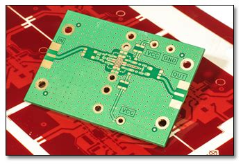
What is PCB Prototyping?
PCB prototyping is the process of creating a small number of printed circuit boards for testing and validation purposes before mass production. The goal of PCB prototyping is to ensure that the design meets the required specifications, functions as intended, and is ready for full-scale manufacturing. Prototyping allows designers and engineers to identify and rectify any issues or errors in the design, ultimately saving time and money in the long run.
Benefits of PCB Prototyping
- Design validation: Prototyping enables designers to test and validate their PCB designs in real-world scenarios, ensuring that the board functions as expected.
- Error identification: By creating prototypes, designers can identify and correct any errors or issues in the design before proceeding with mass production.
- Cost-effective: Prototyping helps avoid costly mistakes and redesigns that may arise during mass production, ultimately saving money and resources.
- Time-saving: By identifying and rectifying issues early in the design process, prototyping can significantly reduce the overall development time of a product.
The PCB CAM Process
The PCB CAM process is a critical stage in PCB prototyping that bridges the gap between the design and fabrication phases. It involves the use of specialized software to convert the PCB design files into machine-readable instructions for the manufacturing equipment. The CAM process ensures that the design is accurately translated into the physical PCB, taking into account various manufacturing constraints and requirements.
Steps in the PCB CAM Process
- Design import: The PCB design files, usually in Gerber or ODB++ Format, are imported into the CAM software.
- Design verification: The CAM software checks the design for any errors, inconsistencies, or violations of manufacturing constraints.
- Panelization: Multiple PCB designs are arranged on a single panel to optimize material usage and minimize manufacturing costs.
- Tooling and drilling: The CAM software generates the necessary tooling and drilling instructions for the manufacturing equipment.
- Output generation: The final output files, such as Gerber files, drill files, and pick-and-place files, are generated for use in the fabrication process.
Importance of PCB CAM in Prototyping
- Ensures manufacturability: The CAM process verifies that the PCB design can be manufactured using the available equipment and processes, minimizing the risk of production issues.
- Optimizes material usage: Through panelization and other techniques, the CAM process helps optimize the use of materials, reducing waste and lowering production costs.
- Enhances accuracy: By precisely translating the design into machine-readable instructions, the CAM process ensures that the manufactured PCB accurately reflects the original design intent.
- Speeds up prototyping: An efficient CAM process can significantly reduce the time required to create PCB Prototypes, allowing for faster iterations and shorter development cycles.

PCB CAM Software and Tools
There are various PCB CAM software and tools available in the market, each with its own set of features and capabilities. Some of the popular PCB CAM software include:
| Software | Manufacturer | Key Features |
|---|---|---|
| CAMCAD | CAMCAD Systems | Automatic panelization, design verification, 3D visualization |
| CAM350 | DownStream Technologies | Design analysis, panelization, Gerber editing |
| UCAMCO | UCAMCO | Gerber editing, panelization, design rule checking |
| Genesis 2000 | Numerical Innovations | Panelization, NC drill optimization, Gerber editing |
When choosing a PCB CAM software, it is essential to consider factors such as compatibility with your existing design tools, ease of use, and the specific features required for your prototyping needs.

Best Practices for PCB CAM in Prototyping
To ensure a smooth and successful PCB CAM process during prototyping, consider the following best practices:
- Maintain clear communication between the design and manufacturing teams to avoid misinterpretations and errors.
- Adhere to the manufacturer’s design guidelines and constraints to minimize the risk of production issues.
- Use standard file formats, such as Gerber or ODB++, to ensure compatibility with the CAM software and manufacturing equipment.
- Perform thorough design verification and rule checks to identify and correct any errors or violations before proceeding with the CAM process.
- Optimize panelization and material usage to reduce costs and waste during prototyping.

FAQ
-
Q: What is the difference between PCB design and PCB CAM?
A: PCB design focuses on creating the schematic and layout of the printed circuit board, while PCB CAM involves translating the design files into machine-readable instructions for manufacturing. -
Q: Can I use the same software for both PCB design and CAM?
A: While some software packages offer both design and CAM capabilities, it is more common to use separate specialized tools for each stage of the process. -
Q: How long does the PCB CAM process typically take?
A: The duration of the PCB CAM process can vary depending on the complexity of the design and the efficiency of the CAM software and operator. However, it generally takes a few hours to a few days to complete the CAM process for a typical PCB prototype. -
Q: What are the most common file formats used in PCB CAM?
A: The most common file formats used in PCB CAM are Gerber (RS-274X) and ODB++ (Open Database++). These formats contain all the necessary information for manufacturing, including layer data, drill data, and component placement. -
Q: How can I ensure the success of my PCB prototyping project?
A: To ensure the success of your PCB prototyping project, follow best practices such as maintaining clear communication, adhering to design guidelines, using standard file formats, performing thorough design verification, and optimizing panelization and material usage. Additionally, choose a reliable PCB manufacturer with experience in prototyping and a robust CAM process.
In conclusion, the PCB CAM process plays a vital role in the success of PCB prototyping projects. By accurately translating the design into machine-readable instructions, optimizing material usage, and ensuring manufacturability, the CAM process helps create high-quality PCB Prototypes that meet the required specifications and functionality. By understanding the importance of PCB CAM and following best practices, designers and engineers can streamline their prototyping efforts and bring their products to market faster and more efficiently.
No responses yet