Introduction to PCB Fabrication
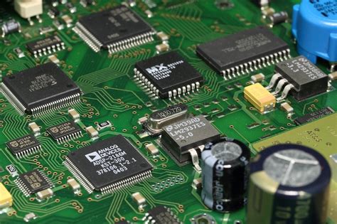
Printed Circuit Boards (PCBs) are the backbone of modern electronics. They are used in almost every electronic device, from simple gadgets to complex machines. PCB fabrication is the process of creating these boards, which involves designing, printing, and etching the circuit pattern onto a substrate material.
While PCB fabrication is typically done in specialized factories, it is possible to make PCBs at home with the right tools and techniques. In this article, we will explore an easy approach to make PCBs at home that can be helpful for hobbyists, students, and anyone interested in electronics.
What You Need for Home PCB Fabrication
Before we dive into the process of making PCBs at home, let’s take a look at the materials and tools you will need:
Materials:
- Copper clad board (PCB substrate)
- Etch-resistant marker or transfer paper
- Ferric chloride or other etching solution
- Acetone or other cleaning solution
- Drill bits (for making holes)
Tools:
- Laser printer or photocopy machine
- UV exposure unit (optional)
- Etching tank or container
- Drill or drill press
- Safety gear (gloves, goggles, respirator)
With these materials and tools, you can create your own PCBs at home. Let’s take a closer look at each step of the process.

Step 1: Design Your PCB
The first step in making a PCB is to design the circuit. You can use various software tools for this purpose, such as Eagle, KiCad, or Fritzing. These tools allow you to create a schematic diagram of your circuit and then convert it into a PCB layout.
When designing your PCB, keep in mind the following considerations:
- Component placement: Arrange the components in a logical and efficient manner to minimize the length of traces and avoid interference.
- Trace width: Choose appropriate trace widths based on the current carrying capacity and impedance requirements of your circuit.
- Clearance: Ensure adequate clearance between traces, pads, and components to avoid short circuits and manufacturability issues.
- Drill holes: Add drill holes for through-hole components and mounting purposes.
Once you have completed the PCB design, export the Gerber files, which contain the necessary information for fabricating the board.

Step 2: Print the PCB Artwork
The next step is to transfer the PCB artwork onto the copper clad board. There are two common methods for doing this:
Method 1: Toner Transfer
- Print the PCB artwork onto a glossy paper using a laser printer. Make sure to print a mirrored image of the artwork.
- Clean the copper clad board with acetone to remove any grease or oxidation.
- Place the printed artwork face down onto the copper side of the board and secure it with tape.
- Use a clothes iron set to high heat (no steam) to press the paper onto the board for several minutes. Apply firm and even pressure.
- Allow the board to cool and then carefully peel off the paper. The toner should have transferred onto the copper surface.
Method 2: UV Exposure
- Print the PCB artwork onto a transparency film using a laser printer or photocopy machine.
- Apply a thin layer of UV-sensitive resist onto the copper clad board using a pre-sensitized board or a resist pen.
- Place the transparency film onto the resist-coated board and secure it with glass or acrylic sheet.
- Expose the board to UV light for the recommended time (usually a few minutes).
- Develop the board in a sodium hydroxide solution to remove the unexposed resist.
Here’s a comparison of the two methods:
| Method | Advantages | Disadvantages |
|---|---|---|
| Toner Transfer | – Inexpensive – No special equipment needed |
– Limited resolution – Requires practice to get consistent results |
| UV Exposure | – High resolution – Consistent results |
– Requires UV exposure unit – More expensive materials |
Choose the method that best suits your needs and resources.

Step 3: Etch the PCB
After transferring the PCB artwork onto the copper clad board, the next step is to etch away the unwanted copper to form the circuit traces. The most common etching solution used for home PCB fabrication is ferric chloride.
- Prepare the etching solution according to the manufacturer’s instructions. Wear gloves and goggles when handling the solution.
- Place the board into the etching tank or container, ensuring that it is completely submerged in the solution.
- Agitate the solution periodically to promote even etching. You can use an aquarium pump or a magnetic stirrer for this purpose.
- Monitor the etching process until all the unwanted copper has been removed. This may take anywhere from 10 to 45 minutes, depending on the strength of the solution and the thickness of the copper.
- Remove the board from the solution and rinse it thoroughly with water.
Step 4: Clean and Drill the PCB
After etching, you will need to clean the board and drill holes for the components.
- Use acetone or a PCB cleaner solution to remove the etch resist from the board. This will reveal the shiny copper traces.
- Inspect the board for any defects or shorts. Use a multimeter to check for continuity between the traces.
- Drill holes for the components using a drill or drill press. Use the appropriate drill bit size for each component.
- Clean the board again to remove any debris from drilling.
Step 5: Solder the Components
The final step is to solder the components onto the PCB.
- Place the components onto the board, ensuring that they are aligned with the drill holes.
- Secure the components in place using masking tape or a holding jig.
- Apply flux to the component leads and pads to promote better soldering.
- Heat up the soldering iron and apply a small amount of solder to the tip to tin it.
- Touch the soldering iron to the component lead and pad simultaneously, allowing the solder to flow and form a joint. Avoid applying too much solder, as this can cause bridges between the traces.
- Repeat the process for all the components until the board is fully assembled.
Conclusion
Making PCBs at home can be a fun and rewarding experience for anyone interested in electronics. By following the easy approach outlined in this article, you can create your own custom PCBs using readily available materials and tools.
Remember to always prioritize safety when working with chemicals and power tools. Wear appropriate safety gear and work in a well-ventilated area.
With practice and patience, you can produce high-quality PCBs that rival those made in professional factories. So go ahead and give it a try! Your next electronics project awaits.
FAQ
Q: How long does it take to make a PCB at home?
A: The total time to make a PCB at home depends on various factors, such as the complexity of the design, the etching method used, and the skill level of the maker. On average, a simple PCB can be made in a few hours, while more complex boards may take a day or two.
Q: Can I use any type of paper for the toner transfer method?
A: No, regular paper will not work for the toner transfer method. You need to use glossy paper or special PCB transfer paper that has a smooth surface and can withstand the heat of the iron. Using the wrong type of paper will result in poor transfer of the artwork onto the copper board.
Q: How long does it take for the ferric chloride solution to etch the board?
A: The etching time depends on the strength of the ferric chloride solution and the thickness of the copper layer on the board. A fresh, concentrated solution can etch a board in 10-15 minutes, while a weaker or exhausted solution may take up to 45 minutes or more. It’s important to monitor the etching process closely to avoid over-etching the board.
Q: What should I do if there are defects or shorts on the PCB after etching?
A: If you notice any defects or shorts on the PCB after etching, you can try to repair them using a few techniques:
- For small breaks in the traces, use a conductive ink pen or a fine-tipped soldering iron to bridge the gap.
- For larger defects, you can cut out the damaged area using a knife or rotary tool and then patch it with a piece of copper tape or wire.
- For shorts between the traces, use a knife or scalpel to carefully scrape away the excess copper until the short is removed.
If the defects are too extensive, it may be easier to start over with a new board.
Q: Can I reuse the ferric chloride solution for multiple boards?
A: Yes, you can reuse the ferric chloride solution for etching multiple boards. However, the solution will become less effective over time as it dissolves more copper. You can extend the life of the solution by regularly filtering out the copper sludge and adding fresh ferric chloride. When the solution becomes too weak or contaminated, dispose of it properly according to your local regulations and make a new batch.
No responses yet