What is a JFET?
A JFET is a type of field-effect transistor that uses a voltage applied to a gate terminal to control the current flow between the source and drain terminals. Unlike bipolar junction transistors (BJTs), JFETs are voltage-controlled devices and offer several advantages, such as high input impedance and low noise.
Types of JFETs
There are two main types of JFETs:
-
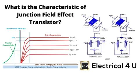
N-channel JFET: In an n-channel JFET, the current carriers are electrons, and the device is normally on (conducts) when the gate-to-source voltage (VGS) is zero.
-
P-channel JFET: In a p-channel JFET, the current carriers are holes, and the device is normally on when VGS is zero.
The J111 is an n-channel JFET.
J111 JFET Pinout
The J111 JFET has three terminals: gate (G), drain (D), and source (S). The pinout of the J111 JFET in a TO-92 package is as follows:
| Pin | Symbol | Description |
|---|---|---|
| 1 | G | Gate |
| 2 | D | Drain |
| 3 | S | Source |
It is essential to identify the correct pinout when using the J111 JFET in a circuit to ensure proper functionality and avoid damage to the device.

J111 JFET Features and Characteristics
The J111 JFET exhibits several notable features and characteristics that make it suitable for various applications:
-
High input impedance: The J111 JFET has a high input impedance, typically in the range of 109 to 1012 ohms, which minimizes loading effects on the input signal source.
-
Low noise: JFETs, including the J111, have inherently low noise characteristics compared to BJTs, making them ideal for Low-noise Amplifier applications.
-
Voltage-controlled operation: The J111 JFET is a voltage-controlled device, meaning that the current flowing through the channel is controlled by the voltage applied to the gate terminal.
-
Wide operating temperature range: The J111 JFET can operate over a wide temperature range, typically from -55°C to +125°C, making it suitable for various environmental conditions.
-
High gain-bandwidth product: The J111 JFET offers a high gain-bandwidth product, enabling its use in high-frequency applications.
J111 JFET Electrical Characteristics
The following table summarizes some of the key electrical characteristics of the J111 JFET:
| Parameter | Symbol | Min | Typ | Max | Unit |
|---|---|---|---|---|---|
| Gate-to-Source Cutoff Voltage | VGS(off) | -5 | -2.5 | -1 | V |
| Zero Gate Voltage Drain Current | IDSS | 2 | 10 | 20 | mA |
| Gate-to-Source Leakage Current | IGSS | – | – | 1 | nA |
| Drain-to-Source On-State Resistance | RDS(on) | – | 50 | 200 | Ω |
| Input Capacitance | Ciss | – | 6 | – | pF |
| Transconductance | gm | 2 | 5 | – | mS |
These electrical characteristics provide insights into the performance and limitations of the J111 JFET and are essential for designing circuits that leverage its capabilities.

J111 JFET Applications
The J111 JFET finds applications in various electronic circuits, such as:
-
Low-noise amplifiers: The low noise characteristics of the J111 JFET make it suitable for designing low-noise amplifiers for audio, RF, and instrumentation applications.
-
Voltage-controlled resistors: The J111 JFET can be used as a voltage-controlled resistor, where the resistance between the drain and source terminals is controlled by the gate-to-source voltage.
-
Current sources: The J111 JFET can be configured as a constant current source, providing a stable current over a wide range of load impedances.
-
Switching circuits: The J111 JFET can be used as a voltage-controlled switch, offering high isolation and low leakage currents.
-
Oscillators: The J111 JFET can be employed in oscillator circuits, such as Colpitts and Hartley Oscillators, to generate sinusoidal or square wave signals.
Example Circuit: J111 JFET Low-Noise Amplifier
One common application of the J111 JFET is in low-noise amplifier circuits. The following schematic shows a simple J111 JFET low-noise amplifier:
           R1
           |
           |
Vin --- C1 --- G
               |
               |          R3
               |           |
               S --- R2 --- +
               |           |
               |          --- C2
              ---
               -
In this circuit:
– R1 is the gate bias resistor, which sets the operating point of the J111 JFET.
– C1 is the input coupling capacitor, which blocks DC and passes the AC input signal.
– R2 is the source resistor, which provides negative feedback and stabilizes the operating point.
– R3 is the drain load resistor, which converts the drain current into an output voltage.
– C2 is the output coupling capacitor, which blocks DC and passes the amplified AC signal.
The values of the components depend on the specific application requirements, such as gain, bandwidth, and input/output impedance.

Frequently Asked Questions (FAQs)
-
What is the difference between a JFET and a MOSFET?
A JFET (Junction Field Effect Transistor) and a MOSFET (Metal-Oxide-Semiconductor Field Effect Transistor) are both voltage-controlled devices. However, a JFET has a reverse-biased PN junction as the gate, while a MOSFET has an insulated gate made of metal oxide. JFETs typically have higher input impedance and lower noise than MOSFETs, but MOSFETs offer higher input impedance and lower gate leakage currents. -
Can a J111 JFET be used as a switch?
Yes, a J111 JFET can be used as a voltage-controlled switch. By applying a suitable gate-to-source voltage, the JFET can be switched between its on-state (low resistance) and off-state (high resistance). However, the switching speed of a JFET is generally slower compared to MOSFETs. -
How do I bias a J111 JFET for linear operation?
To bias a J111 JFET for linear operation, you need to set the operating point by selecting appropriate values for the gate bias resistor (R1) and the source resistor (R2). The goal is to ensure that the JFET operates in the saturation region, where the drain current is controlled by the gate-to-source voltage. A common biasing technique is the self-bias configuration, where the gate is connected to the source through a resistor, and the source resistor provides negative feedback to stabilize the operating point. -
What is the maximum gate-to-source voltage for a J111 JFET?
The maximum gate-to-source voltage for a J111 JFET is typically specified in the device’s datasheet. For most J111 JFETs, the maximum gate-to-source voltage is around -35V to -40V. Exceeding this voltage can damage the device by causing breakdown of the gate-to-channel junction. -
Can a J111 JFET be used in high-frequency applications?
Yes, a J111 JFET can be used in high-frequency applications due to its high gain-bandwidth product. However, the performance of the JFET at high frequencies depends on factors such as the input and output capacitances, which can limit the bandwidth. Proper circuit design techniques, such as impedance matching and minimizing Parasitic Capacitances, are essential for optimizing the high-frequency performance of the J111 JFET.
Conclusion
In this article, we have explored the J111 JFET in detail, covering its pinout, features, applications, and other important aspects. The J111 JFET is a versatile device known for its high input impedance, low noise, and voltage-controlled operation, making it suitable for various analog and digital applications. By understanding the characteristics and biasing requirements of the J111 JFET, engineers and hobbyists can effectively utilize this device in their circuits to achieve desired performance and functionality.
No responses yet