Introduction to PWB
Printed Wiring Boards (PWBs), also known as Printed Circuit Boards (PCBs), are the backbone of modern electronic devices. These boards are used to mechanically support and electrically connect electronic components using conductive pathways, tracks, or signal traces etched from copper sheets laminated onto a non-conductive substrate. PWBs have revolutionized the electronics industry by enabling the creation of compact, reliable, and mass-producible electronic devices.
History of PWB
The history of PWBs dates back to the early 20th century. In 1903, Albert Hanson, a German inventor, filed a patent for a method of creating an electrical connection between metal foils on an insulating board. However, it wasn’t until the 1930s that the first practical PWBs were developed. During World War II, the demand for compact and reliable electronic equipment for military applications drove the development of PWBs.
In the 1950s, the introduction of through-hole technology and the use of fiberglass as a substrate material further advanced the capabilities of PWBs. The 1960s saw the emergence of multilayer PWBs, which allowed for more complex circuit designs and higher component densities.
PWB Manufacturing Process
The manufacturing process of PWBs involves several steps, each critical to ensuring the quality and reliability of the final product.
-
Design: The first step in PWB manufacturing is the design phase. Engineers use specialized software to create a digital representation of the circuit, specifying the placement of components, routing of traces, and other design elements.
-
Substrate Preparation: The substrate, typically made of fiberglass or other insulating materials, is cut to the required size and shape. Holes are drilled into the substrate to accommodate through-hole components and vias.
-
Copper Cladding: A thin layer of copper is laminated onto the substrate using heat and pressure. This copper layer will form the conductive pathways of the PWB.
-
Patterning: The desired circuit pattern is transferred onto the copper-clad substrate using a photolithographic process. A photoresist layer is applied to the copper, and the circuit pattern is exposed using UV light. The unexposed areas are then etched away, leaving the desired copper traces.
-
Protective Coating: A protective coating, such as solder mask, is applied to the PWB to insulate and protect the copper traces. This coating also helps to prevent short circuits and improves the durability of the board.
-
Component Assembly: Electronic components are placed onto the PWB and soldered into place. This can be done manually or using automated pick-and-place machines.
-
Testing and Inspection: The assembled PWB undergoes rigorous testing and inspection to ensure proper functionality and adherence to quality standards. This may include visual inspections, automated optical inspections (AOI), and electrical testing.
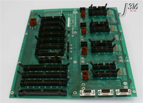
Types of PWBs
There are several types of PWBs, each designed to meet specific requirements and applications.
Single-Layer PWBs
Single-layer PWBs, also known as single-sided PWBs, have conductive traces on only one side of the substrate. These boards are the simplest and most cost-effective type of PWB, suitable for basic electronic circuits with low component densities.
Double-Layer PWBs
Double-layer PWBs, or double-sided PWBs, have conductive traces on both sides of the substrate. The two layers are connected using through-hole vias, allowing for more complex circuit designs and higher component densities compared to single-layer PWBs.
Multilayer PWBs
Multilayer PWBs consist of three or more conductive layers separated by insulating layers. These boards offer the highest level of circuit complexity and component density, making them suitable for advanced electronic applications, such as smartphones, computers, and aerospace systems. Multilayer PWBs can have up to 50 or more layers, depending on the specific requirements of the application.
Flexible PWBs
Flexible PWBs, or flex circuits, are designed to bend and flex without damaging the conductive traces or components. These boards are made using flexible substrate materials, such as polyimide or polyester, and are often used in applications where space is limited, or where the Electronic Assembly needs to conform to a specific shape, such as in wearable devices, medical implants, and automotive electronics.
Rigid-Flex PWBs
Rigid-flex PWBs combine the benefits of both rigid and flexible PWBs. These boards consist of rigid sections, similar to traditional PWBs, connected by flexible sections. This allows for the creation of three-dimensional electronic assemblies that can be folded or shaped to fit into compact spaces, while still maintaining the reliability and durability of rigid PWBs.

PWB Materials
The choice of materials used in PWB manufacturing plays a critical role in determining the performance, reliability, and cost of the final product.
Substrate Materials
The most common substrate materials used in PWB manufacturing are:
-
FR-4: A fiberglass-reinforced epoxy laminate, FR-4 is the most widely used substrate material for PWBs. It offers good mechanical strength, electrical insulation, and thermal stability.
-
Polyimide: Polyimide is a high-performance polymer used in flexible PWBs and high-temperature applications. It offers excellent thermal stability, chemical resistance, and mechanical strength.
-
Teflon: Teflon, or PTFE (polytetrafluoroethylene), is a low-dielectric-constant material used in high-frequency and microwave applications. It offers excellent electrical insulation and thermal stability.
-
Ceramic: Ceramic substrates, such as alumina (Al2O3) and aluminum nitride (AlN), are used in high-power and high-temperature applications. They offer excellent thermal conductivity and electrical insulation.
Conductive Materials
The most common conductive materials used in PWB manufacturing are:
-
Copper: Copper is the most widely used conductive material in PWBs due to its excellent electrical conductivity, thermal conductivity, and mechanical strength. It is typically used in the form of thin foils laminated onto the substrate.
-
Silver: Silver is sometimes used as a conductive material in PWBs due to its high electrical conductivity. However, it is more expensive than copper and is typically used in specialized applications.
-
Gold: Gold is used as a finish for contact pads and connectors in PWBs. It offers excellent corrosion resistance and electrical conductivity, but is more expensive than other conductive materials.

PWB Design Considerations
Designing a PWB involves several key considerations to ensure optimal performance, reliability, and manufacturability.
Signal Integrity
Signal integrity refers to the quality of the electrical signals transmitted through the PWB. Factors that can affect signal integrity include:
- Trace geometry (width, thickness, and spacing)
- Dielectric constant and loss tangent of the substrate material
- Impedance matching
- Crosstalk between adjacent traces
- Electromagnetic interference (EMI)
Designers must carefully consider these factors and employ techniques such as impedance control, differential signaling, and proper grounding to maintain signal integrity.
Thermal Management
Thermal management is critical in PWB design to ensure that the electronic components operate within their specified temperature ranges. Factors that can affect thermal management include:
- Power dissipation of components
- Thermal conductivity of the substrate material
- Placement and spacing of components
- Use of thermal vias and heat sinks
Designers must employ thermal simulation tools and follow best practices for component placement and thermal management to prevent overheating and ensure reliable operation.
Manufacturability
Designing a PWB for manufacturability is essential to ensure that the board can be efficiently and reliably produced. Factors that can affect manufacturability include:
- Minimum feature sizes (trace width, spacing, and hole size)
- Aspect ratios of vias and through-holes
- Solder mask and silkscreen design
- Component placement and orientation
- Panelization and routing
Designers must adhere to manufacturing guidelines and work closely with PWB fabricators to ensure that the design is optimized for manufacturability and cost-effectiveness.

PWB Testing and Inspection
Testing and inspection are critical steps in the PWB manufacturing process to ensure the quality and reliability of the final product.
Visual Inspection
Visual inspection is the first level of quality control in PWB manufacturing. Trained operators visually examine the boards for defects such as:
- Incomplete or excessive solder joints
- Damaged or missing components
- Incorrect component placement or orientation
- Solder bridges or short circuits
- Contamination or foreign objects
Visual inspection can be performed manually or using automated optical inspection (AOI) systems, which use cameras and image processing algorithms to detect defects.
Automated Optical Inspection (AOI)
AOI systems are widely used in PWB manufacturing for high-speed, high-precision inspection of solder joints, component placement, and other critical features. These systems can detect defects that are difficult or impossible to see with the naked eye, such as:
- Solder joint size and shape
- Component polarity and alignment
- Trace width and spacing
- Solder mask and silkscreen accuracy
AOI systems can significantly improve the efficiency and reliability of PWB inspection, reducing the need for manual inspection and catching defects early in the manufacturing process.
Electrical Testing
Electrical testing is performed to verify the electrical functionality and performance of the PWB. Common electrical tests include:
- Continuity testing: Verifies that the conductive paths are properly connected and free of open circuits.
- Insulation testing: Ensures that there are no short circuits between adjacent traces or components.
- Resistance testing: Measures the resistance of traces and components to ensure they are within specified tolerances.
- Functional testing: Verifies that the PWB performs its intended function under various operating conditions.
Electrical testing can be performed using a variety of methods, such as flying probe testing, bed-of-nails testing, and functional test fixtures.
PWB Applications
PWBs are used in a wide range of electronic applications, from consumer devices to industrial equipment and aerospace systems. Some common applications include:
- Consumer electronics: Smartphones, laptops, tablets, televisions, and home appliances
- Automotive electronics: Engine control units, infotainment systems, and advanced driver assistance systems (ADAS)
- Medical devices: Implantable devices, diagnostic equipment, and patient monitoring systems
- Industrial automation: Programmable logic controllers (PLCs), sensors, and automation systems
- Aerospace and defense: Avionics, radar systems, and satellite communications
- Telecommunications: Routers, switches, and base stations
The specific requirements for PWBs in each application vary depending on factors such as operating environment, performance requirements, and cost constraints. PWB designers and manufacturers must work closely with their customers to ensure that the boards meet the specific needs of each application.
Future Trends in PWB Technology
As electronic devices continue to become more complex and demand for high-performance, compact, and cost-effective solutions grows, PWB technology must continue to evolve to keep pace. Some of the key trends shaping the future of PWB technology include:
Advanced Materials
Researchers are continuously developing new substrate and conductive materials to improve the performance and reliability of PWBs. Some examples include:
- High-frequency laminates with low dielectric constant and loss tangent for 5G and millimeter-wave applications
- Graphene-based conductive inks for printed electronics and flexible PWBs
- Ceramic and metal matrix composite substrates for high-temperature and high-power applications
Embedded Components
Embedding active and passive components within the layers of a PWB can significantly reduce the size and weight of electronic assemblies while improving performance and reliability. Embedded component technologies, such as embedded capacitors, resistors, and integrated circuits (ICs), are becoming increasingly common in advanced PWB designs.
3D Printing
3D printing, or additive manufacturing, is emerging as a promising technology for PWB fabrication. 3D printing enables the creation of complex, three-dimensional structures with intricate geometries and embedded components, which are difficult or impossible to achieve with traditional manufacturing methods. This technology has the potential to revolutionize PWB design and manufacturing, enabling faster prototyping, greater design flexibility, and reduced waste.
Artificial Intelligence (AI) in Design and Manufacturing
AI and machine learning algorithms are being applied to various aspects of PWB design and manufacturing, from design automation and optimization to quality control and predictive maintenance. AI-driven tools can help designers create more efficient and reliable PWB layouts, identify potential manufacturability issues, and optimize production processes for improved quality and throughput.
Sustainability and Eco-Friendly Practices
As environmental concerns continue to grow, the PWB industry is focusing on developing more sustainable and eco-friendly manufacturing practices. This includes the use of lead-free solders, halogen-free laminates, and recyclable materials, as well as the adoption of energy-efficient production processes and waste reduction strategies.
Conclusion
PWBs have come a long way since their inception in the early 20th century, evolving into the complex, high-performance, and ubiquitous components that power our modern electronic devices. As technology continues to advance and new applications emerge, PWB designers and manufacturers must stay at the forefront of innovation, embracing new materials, manufacturing processes, and design tools to meet the ever-growing demands of the electronics industry.
By understanding the fundamentals of PWB technology, including manufacturing processes, materials, design considerations, and testing and inspection methods, engineers and technicians can create reliable, high-performance electronic assemblies that drive innovation across a wide range of industries.
As the world becomes increasingly connected and reliant on electronic devices, the importance of PWBs will only continue to grow. By staying informed about the latest trends and advancements in PWB technology, professionals in the electronics industry can position themselves for success in this dynamic and rapidly evolving field.
Frequently Asked Questions (FAQ)
-
What is the difference between a PWB and a PCB?
PWB (Printed Wiring Board) and PCB (Printed Circuit Board) are often used interchangeably, as they refer to the same type of board. However, some professionals make a distinction based on the manufacturing process: PWBs are created by printing conductive traces on the substrate, while PCBs are created by etching away unwanted copper from a fully clad substrate. -
What are the advantages of using a multilayer PWB?
Multilayer PWBs offer several advantages over single- and double-layer boards, including: - Higher component density and more complex circuit designs
- Improved signal integrity and reduced electromagnetic interference (EMI)
- Better thermal management and power distribution
-
Reduced overall size and weight of the electronic assembly
-
What is the purpose of solder mask on a PWB?
Solder mask is a protective coating applied to the copper traces on a PWB. It serves several purposes: - Insulates and protects the copper traces from oxidation and corrosion
- Prevents solder bridging and short circuits during component assembly
- Provides a visual contrast for easier component placement and inspection
-
Improves the aesthetic appearance of the board
-
What is the difference between through-hole and surface-mount components?
Through-hole components have leads that are inserted into holes drilled in the PWB and soldered on the opposite side. Surface-mount components are placed directly on the surface of the PWB and soldered in place. Surface-mount components are smaller and allow for higher component densities, while through-hole components are more robust and easier to replace. -
What is the role of impedance control in PWB design?
Impedance control is a critical aspect of PWB design, particularly for high-speed and high-frequency applications. By carefully controlling the geometry and spacing of the conductive traces, designers can ensure that the characteristic impedance of the traces matches the impedance of the components and connectors. This helps to minimize signal reflections, distortions, and crosstalk, ensuring reliable signal transmission and overall system performance.
No responses yet