PCB Fabrication
PCB fabrication is the process of creating the bare circuit board that will later be populated with electronic components during the assembly phase. The fabrication process involves several steps, including:
1. Design and Layout
The first step in PCB fabrication is designing the circuit board using specialized software, such as Eagle, Altium Designer, or KiCad. The design includes the placement of components, traces, and vias, as well as the creation of the necessary layers for the board.
2. Material Selection
The most common material used for PCBs is FR-4, a glass-reinforced epoxy laminate. Other materials, such as polyimide or ceramic, may be used for specific applications that require higher heat resistance or better electrical properties.
3. Copper Cladding
A thin layer of copper is bonded to the substrate material using heat and pressure. The copper layer will form the conductive traces on the PCB.
4. Drilling
Holes are drilled through the board to accommodate through-hole components and to create vias that connect different layers of the PCB.
5. Patterning
The desired circuit pattern is transferred onto the copper layer using a photoresist and exposure to UV light. The exposed areas are then etched away, leaving only the desired copper traces.
6. Plating
The board is plated with a thin layer of copper to protect the exposed traces and to provide a better surface for soldering. Additional finishes, such as gold, silver, or nickel, may be applied depending on the specific requirements of the project.
7. Solder Mask Application
A solder mask, typically green in color, is applied to the board to protect the copper traces from oxidation and to prevent solder bridges during the assembly process.
8. Silkscreen
A silkscreen layer is added to the board to provide labels, logos, and other identifying marks. This layer helps with the assembly process and makes it easier to identify components and their placement.
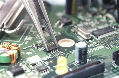
PCB Assembly
PCB assembly, also known as PCBA (Printed Circuit Board Assembly), is the process of populating the fabricated circuit board with electronic components. The assembly process can be broken down into several steps:
1. Solder Paste Application
Solder paste, a mixture of tiny solder particles and flux, is applied to the pads on the PCB where components will be placed. This is typically done using a stencil and a solder paste printer.
2. Component Placement
Surface mount components are placed onto the solder paste using a pick-and-place machine. This machine uses vacuum nozzles to pick up components from reels or trays and place them accurately on the board.
3. Reflow Soldering
The board is then passed through a reflow oven, which heats the solder paste to its melting point. As the solder cools, it forms a strong mechanical and electrical bond between the components and the PCB.
4. Through-Hole Component Insertion
If the board includes through-hole components, they are inserted manually or using automated insertion machines.
5. Wave Soldering
For boards with through-hole components, a wave soldering machine is used to apply solder to the underside of the board. The board is passed over a wave of molten solder, which fills the through-holes and creates a strong connection.
6. Inspection and Testing
After the soldering process, the assembled boards are inspected visually and tested using various methods, such as in-circuit testing (ICT), boundary scan testing, or functional testing. This ensures that the board is functioning correctly and meets the required specifications.
7. Conformal Coating and Potting
In some cases, a conformal coating or potting compound may be applied to the assembled board to protect it from environmental factors such as moisture, dust, or mechanical stress.

Differences between PCB Fabrication and Assembly
While PCB fabrication and assembly are both essential processes in the production of electronic devices, they differ in several key aspects:
-
Process Focus: PCB fabrication focuses on creating the bare circuit board, while assembly focuses on populating the board with components.
-
Equipment: Fabrication requires equipment such as UV exposure units, etching machines, and plating tanks, while assembly relies on pick-and-place machines, reflow ovens, and wave soldering machines.
-
Materials: Fabrication primarily deals with substrate materials, copper, and photoresists, while assembly involves solder paste, electronic components, and conformal coatings.
-
Skills: PCB fabrication requires expertise in chemical processes, photolithography, and material science, while assembly relies on knowledge of component placement, soldering techniques, and quality control.
-
Time and Cost: Fabrication is generally more time-consuming and expensive than assembly, as it involves more complex processes and requires specialized equipment.

Importance of PCB Fabrication and Assembly
Both PCB fabrication and assembly play crucial roles in the production of electronic devices. Without a well-designed and fabricated PCB, the electronic components would have no platform to be assembled on. Similarly, without proper assembly, even the most well-fabricated PCB would be useless.
High-quality PCB fabrication ensures that the circuit board has the correct dimensions, hole placements, and conductive traces. This is essential for the proper functioning of the electronic device and helps to minimize issues such as signal interference, crosstalk, and power loss.
Precise PCB assembly guarantees that components are placed accurately and soldered correctly, which is critical for the reliability and longevity of the electronic device. Poor assembly can lead to issues such as cold solder joints, bridging, or component misalignment, which can cause device failure or malfunction.

Comparison Table: PCB Fabrication vs. Assembly
| Aspect | PCB Fabrication | PCB Assembly |
|---|---|---|
| Focus | Creating the bare circuit board | Populating the board with components |
| Equipment | UV exposure units, etching machines, plating tanks | Pick-and-place machines, reflow ovens, wave soldering machines |
| Materials | Substrate materials, copper, photoresists | Solder paste, electronic components, conformal coatings |
| Skills | Chemical processes, photolithography, material science | Component placement, soldering techniques, quality control |
| Time and Cost | More time-consuming and expensive | Less time-consuming and expensive |
Frequently Asked Questions (FAQ)
-
Q: Can the same company handle both PCB fabrication and assembly?
A: Yes, many companies offer both PCB fabrication and assembly services, which is known as a turnkey solution. This can simplify the process for customers and ensure better compatibility between the fabricated board and the assembled components. -
Q: What is the difference between surface mount and through-hole components?
A: Surface mount components are placed directly on the surface of the PCB and soldered using a reflow process. Through-hole components have leads that are inserted into holes drilled in the PCB and soldered using a wave soldering process. Surface mount components are generally smaller and more suitable for high-density designs, while through-hole components are more robust and easier to replace. -
Q: What is the purpose of a solder mask in PCB fabrication?
A: A solder mask is a layer applied to the PCB during fabrication that serves two main purposes. First, it protects the copper traces from oxidation and corrosion. Second, it prevents solder bridges from forming between adjacent pads during the assembly process, which could cause short circuits. -
Q: How do I choose between PCB fabrication materials?
A: The choice of PCB fabrication material depends on the specific requirements of your project. Factors to consider include the operating temperature range, dielectric constant, thermal conductivity, and cost. For most general-purpose applications, FR-4 is a suitable choice. However, for high-frequency or high-temperature applications, materials like Rogers laminates or polyimide may be more appropriate. -
Q: What is the role of testing in PCB assembly?
A: Testing is a critical step in PCB assembly that ensures the assembled board functions as intended and meets the required specifications. Various testing methods, such as in-circuit testing (ICT), boundary scan testing, and functional testing, can help identify issues like component placement errors, short circuits, or incorrect component values. Testing helps to catch defects early in the production process, reducing costs and improving overall product quality.
In conclusion, PCB fabrication and assembly are two distinct but equally important processes in the production of electronic devices. Fabrication focuses on creating the bare circuit board, while assembly involves populating the board with components. Understanding the differences between these processes, as well as their respective importance, is crucial for anyone involved in the design, manufacture, or procurement of electronic products.
By ensuring high-quality PCB fabrication and assembly, manufacturers can produce reliable, efficient, and cost-effective electronic devices that meet the ever-growing demands of the modern world.
No responses yet