Understanding SMD Components
SMD components are electronic components that are designed to be mounted directly onto the surface of a printed circuit board (PCB). Unlike through-hole components, SMD components do not require holes to be drilled in the PCB, making the assembly process faster and more automated.
Advantages of SMD Components
- Smaller size: SMD components are much smaller than their through-hole counterparts, allowing for more compact designs and higher component density on the PCB.
- Improved performance: Due to their smaller size and shorter lead lengths, SMD components have reduced parasitic inductance and capacitance, resulting in better high-frequency performance.
- Faster assembly: SMD components can be placed and soldered onto the PCB using automated equipment, significantly reducing assembly time and costs.
- Increased reliability: SMD components have a lower profile and are less susceptible to mechanical stress, vibrations, and shock, leading to improved reliability.
Common SMD Component Packages
SMD components come in various packages, each with its own size, shape, and lead configuration. Some of the most common SMD Packages include:
| Package | Description | Dimensions (mm) |
|---|---|---|
| 0201 | Smallest commercially available package | 0.6 x 0.3 |
| 0402 | Widely used for passive components | 1.0 x 0.5 |
| 0603 | Popular for resistors and capacitors | 1.6 x 0.8 |
| 0805 | Larger package for higher power dissipation | 2.0 x 1.25 |
| 1206 | Used for high-power resistors and capacitors | 3.2 x 1.6 |
| SOIC | Small Outline Integrated Circuit, used for ICs | Various sizes |
| QFP | Quad Flat Package, used for microcontrollers and ICs | Various sizes |
| BGA | Ball Grid Array, used for high-density ICs | Various sizes |
SMD Assembly Process
The SMD assembly process involves several steps, from PCB preparation to final inspection. The following sections will guide you through each stage of the process.
PCB Preparation
- Design the PCB layout: Ensure that the PCB layout is optimized for SMD assembly, with appropriate pad sizes, spacing, and solder mask openings.
- Apply solder paste: Use a solder paste stencil to apply solder paste onto the PCB pads. The stencil ensures that the correct amount of solder paste is deposited on each pad.
- Inspect solder paste: Use a solder paste inspection (SPI) system to check the quality and consistency of the solder paste deposits.
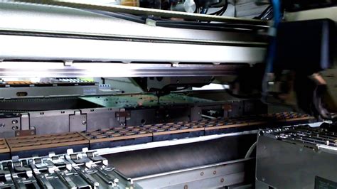
Component Placement
- Load components: Load the SMD components onto the pick-and-place machine feeders or trays, ensuring that the correct components are used for each location on the PCB.
- Place components: The pick-and-place machine uses a vacuum nozzle to pick up the SMD components and place them accurately on the PCB pads.
- Inspect placement: Use an automated optical inspection (AOI) system to verify that the components are placed correctly and that there are no missing or misaligned components.
Reflow Soldering
- Preheat the PCB: Place the PCB with the placed components into a reflow oven. The preheating stage gradually raises the temperature of the PCB and components to prevent thermal shock.
- Reflow solder: As the temperature increases, the solder paste melts and forms a strong bond between the component leads and the PCB pads. The reflow profile must be carefully controlled to ensure optimal solder joint formation.
- Cool down: After the reflow soldering process, the PCB is cooled down gradually to room temperature to prevent thermal stress and warping.
Inspection and Testing
- Visual inspection: Perform a visual inspection of the assembLED PCB to check for any visible defects, such as bridging, tombstoning, or insufficient solder.
- X-ray inspection: Use X-ray inspection to check for hidden defects, such as voids in the solder joints or misaligned BGA components.
- Functional testing: Perform functional tests to ensure that the assembled PCB operates as intended and meets the required specifications.

Common SMD Assembly Defects and Solutions
Despite careful process control, SMD assembly defects can still occur. Identifying and addressing these defects is crucial for ensuring the quality and reliability of the assembled PCBs.
Bridging
Bridging occurs when excess solder creates an unintended connection between two or more adjacent pads or leads.
Solutions:
– Adjust the solder paste stencil aperture size to control the amount of solder paste deposited.
– Optimize the reflow profile to ensure proper solder melting and wetting.
– Use a solder mask to prevent solder from flowing between closely spaced pads.
Tombstoning
Tombstoning, also known as the Manhattan effect, occurs when one end of a component lifts off the PCB pad during the reflow soldering process.
Solutions:
– Ensure that the solder paste is applied evenly on both pads.
– Optimize the reflow profile to minimize the temperature difference between the component leads.
– Use components with a larger pad-to-lead ratio to improve stability during reflow.
Insufficient Solder
Insufficient solder can result in weak or open connections between the component leads and the PCB pads.
Solutions:
– Increase the solder paste stencil aperture size to deposit more solder paste.
– Ensure that the solder paste is stored and handled properly to maintain its quality.
– Verify that the reflow profile provides adequate time and temperature for solder melting and wetting.
Component Shift
Component shift occurs when a component moves from its intended position during the reflow soldering process.
Solutions:
– Ensure that the solder paste is applied evenly on the pads to provide a balanced force on the component.
– Optimize the pick-and-place machine settings to achieve accurate component placement.
– Use a solder mask to create a barrier that helps maintain component position during reflow.

Best Practices for SMD Assembly
To ensure a successful and efficient SMD assembly process, consider implementing the following best practices:
- Use high-quality materials: Invest in high-quality solder paste, SMD components, and PCBs to minimize defects and improve reliability.
- Implement process control: Monitor and control the critical parameters of each assembly stage, such as solder paste deposition, component placement, and reflow soldering.
- Regularly maintain equipment: Perform regular maintenance and calibration of the assembly equipment to ensure consistent performance and accuracy.
- Train personnel: Provide adequate training to the assembly personnel to ensure that they follow the correct procedures and best practices.
- Continuously improve: Regularly review and analyze the assembly process to identify areas for improvement and implement necessary changes.

Frequently Asked Questions (FAQ)
- What is the difference between SMD and through-hole components?
-
SMD components are designed to be mounted directly onto the surface of a PCB, while through-hole components require holes to be drilled in the PCB for their leads to pass through.
-
Can SMD components be soldered manually?
-
Yes, SMD components can be soldered manually using a fine-tipped soldering iron and tweezers. However, manual soldering is more time-consuming and requires a steady hand and good eyesight.
-
What is the purpose of solder paste in SMD assembly?
-
Solder paste is a mixture of tiny solder particles suspended in a flux medium. It is used to temporarily hold the SMD components in place on the PCB pads and provide the necessary solder for creating a strong bond during the reflow soldering process.
-
How can I prevent tombstoning during SMD assembly?
-
To prevent tombstoning, ensure that the solder paste is applied evenly on both pads, optimize the reflow profile to minimize temperature differences between the component leads, and use components with a larger pad-to-lead ratio for improved stability.
-
What is the role of AOI in SMD assembly?
- Automated Optical Inspection (AOI) is used to verify that the SMD components are placed correctly on the PCB and that there are no missing or misaligned components. AOI systems use high-resolution cameras and advanced image processing algorithms to detect assembly defects quickly and accurately.
In conclusion, SMD assembly is a critical process in the electronics manufacturing industry, enabling the production of smaller, faster, and more reliable electronic devices. By understanding the SMD assembly process, common defects, and best practices, manufacturers can ensure a high-quality and efficient assembly process. Regular monitoring, maintenance, and continuous improvement are essential for achieving optimal results and staying competitive in the ever-evolving electronics market.
No responses yet