What is a Flexible PCB?
A flexible PCB, also known as a flex circuit or FPC, is a printed circuit board made from flexible materials, such as polyimide or polyester. Unlike Rigid PCBs, which are made from a solid substrate, FPCs can bend and twist without breaking or losing their electrical properties. This makes them ideal for applications where space is limited, or where the PCB needs to conform to a specific shape.
Advantages of Flexible PCBs
- Lightweight and compact
- Able to withstand vibration and shock
- Reduced assembly time and costs
- Improved electrical performance
- Increased design flexibility
Flexible PCB Manufacturing Process Overview
The manufacturing process for flexible PCBs involves several key steps:
- Circuit Design
- Material Selection
- Printing and Etching
- Lamination
- Drilling and Cutting
- Surface Finish
- Solder Mask Application
- Silkscreen Printing
- Electrical Testing
- Final Assembly
Let’s dive into each step in more detail.
Step 1: Circuit Design
The first step in the FlexPCBFab process is designing the circuit. This involves creating a schematic diagram and a layout of the circuit using CAD (Computer-Aided Design) software. The design must consider the specific requirements of the application, such as the size, shape, and number of layers needed.
Step 2: Material Selection
Choosing the right materials is crucial for ensuring the performance and reliability of the flexible PCB. The most common materials used for FPCs are:
- Polyimide (PI): A high-temperature, chemically resistant polymer with excellent mechanical and electrical properties.
- Polyester (PET): A lower-cost alternative to PI, suitable for less demanding applications.
- Adhesives: Used to bond the copper foil to the substrate and the coverlay to the circuit.
| Material | Advantages | Disadvantages |
|---|---|---|
| Polyimide | High-temperature resistance, durability | Higher cost, more difficult to process |
| Polyester | Lower cost, easier to process | Lower temperature resistance, less durable |
| Adhesives | Strong bonding, chemical resistance | Can affect electrical properties if not chosen carefully |
Step 3: Printing and Etching
Once the materials are selected, the next step is to print and etch the circuit pattern onto the copper foil. This is typically done using a photolithographic process:
- The copper foil is coated with a light-sensitive resist.
- The circuit pattern is transferred onto the resist using a photomask and UV light.
- The exposed resist is developed, revealing the copper to be etched away.
- The unwanted copper is removed using a chemical etching process.
- The remaining resist is stripped away, leaving the desired circuit pattern.
Step 4: Lamination
After the circuit pattern is etched, the copper foil is laminated onto the flexible substrate using heat and pressure. The adhesive layer bonds the copper to the substrate, creating a strong and durable bond.
Step 5: Drilling and Cutting
Any necessary holes, such as vias or mounting holes, are drilled into the laminated FPC. The board is then cut to its final shape using a precision cutting machine, such as a laser or die cutter.
Step 6: Surface Finish
A surface finish is applied to the exposed copper to protect it from oxidation and improve its solderability. Common surface finishes for FPCs include:
- ENIG (Electroless Nickel Immersion Gold)
- OSP (Organic Solderability Preservative)
- Immersion Silver
- Immersion Tin
| Surface Finish | Advantages | Disadvantages |
|---|---|---|
| ENIG | Excellent solderability, long shelf life | Higher cost, can cause nickel corrosion |
| OSP | Low cost, easy to apply | Limited shelf life, can affect impedance |
| Immersion Silver | Good solderability, low cost | Can tarnish over time, may require additional processing |
| Immersion Tin | Good solderability, low cost | Can form tin whiskers, limited shelf life |
Step 7: Solder Mask Application
A solder mask is applied to the FPC to protect the copper traces from shorts and damage during assembly. The solder mask is typically a photoimageable polymer that is applied using a screen printing process and then cured using UV light.
Step 8: Silkscreen Printing
Any necessary text, logos, or identifying marks are printed onto the FPC using a silkscreen printing process. This helps with assembly and troubleshooting by clearly labeling components and test points.
Step 9: Electrical Testing
Before the final assembly, the FPC undergoes thorough electrical testing to ensure that all connections are working properly and that there are no shorts or open circuits. This may include:
- Continuity testing
- Insulation resistance testing
- Impedance testing
- High-voltage testing
Step 10: Final Assembly
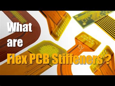
Finally, any necessary components, such as connectors, stiffeners, or heat sinks, are attached to the FPC. The assembled FPC is then packaged and shipped to the customer for integration into their final product.

Frequently Asked Questions (FAQ)
1. What are the most common applications for flexible PCBs?
Flexible PCBs are used in a wide range of applications, including:
- Consumer electronics (smartphones, wearables, laptops)
- Medical devices (hearing aids, pacemakers, endoscopes)
- Automotive electronics (dashboard displays, sensors)
- Aerospace and military equipment (avionics, satellites, missiles)
- Industrial automation (robots, machine vision systems)
2. What are the key differences between rigid and flexible PCBs?
| Characteristic | Rigid PCBs | Flexible PCBs |
|---|---|---|
| Substrate | Solid, typically FR-4 | Flexible, typically polyimide or polyester |
| Thickness | Thicker, 0.8-3.2 mm | Thinner, 0.05-0.3 mm |
| Flexibility | Cannot bend or twist | Can bend, twist, and fold |
| Cost | Lower cost for simple designs | Higher cost, especially for complex designs |
| Assembly | Easier to assemble, more standardized | More challenging, often requires specialized equipment |
3. How do I choose the right material for my flexible PCB?
The choice of material depends on several factors, including:
- Operating temperature range
- Chemical exposure
- Mechanical stress (bending, twisting)
- Electrical requirements (dielectric constant, loss tangent)
- Cost and availability
Work with your FlexPCBFab manufacturer to select the best material for your specific application.
4. What are the most common challenges in flexible PCB manufacturing?
Some of the key challenges in flexible PCB manufacturing include:
- Maintaining dimensional stability during processing
- Ensuring proper adhesion between layers
- Controlling impedance and signal integrity
- Minimizing stress and strain during assembly
- Achieving fine pitch and high-density designs
Experienced FlexPCBFab manufacturers have developed specialized processes and equipment to overcome these challenges and deliver high-quality FPCs.
5. How can I ensure the reliability and longevity of my flexible PCBs?
To maximize the reliability and longevity of your flexible PCBs:
- Use appropriate materials and surface finishes for your application
- Follow best practices for design, such as minimizing bend radii and using strain relief features
- Work with a reputable FlexPCBFab manufacturer with experience in your industry
- Perform thorough testing and qualification of your FPCs before production
- Consider environmental factors, such as temperature, humidity, and vibration, in your design and testing

Conclusion
Flexible PCBs offer unique advantages over rigid PCBs, enabling the development of more compact, lightweight, and versatile electronic devices. However, the manufacturing process for FPCs is more complex and requires specialized materials, equipment, and expertise.
By understanding the key steps in the FlexPCBFab process, from design to final assembly, and working with an experienced manufacturer, you can ensure the successful fabrication of high-quality flexible PCBs for your application.

No responses yet