What is PCB Panelisation?
PCB panelisation is the process of combining multiple small printed circuit boards (PCBs) onto a single large panel for manufacturing. This technique is commonly used to reduce production costs and increase efficiency when producing high volumes of small PCBs. By panelising the boards, manufacturers can optimize material usage, minimize handling, and streamline the assembly process.
Benefits of Panelising PCBs
- Cost reduction: Panelising PCBs allows for the production of multiple boards in a single manufacturing run, reducing setup costs and material waste.
- Increased efficiency: Handling and assembling larger panels is more efficient than dealing with individual small boards.
- Improved quality: Panelisation helps maintain consistent quality across all boards in the panel, as they are subjected to the same manufacturing conditions.
- Simplified logistics: Shipping and handling of panelised PCBs is more convenient and cost-effective compared to individual boards.
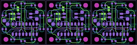
Planning the Panel Layout
Before starting the panelisation process, it is essential to plan the panel layout carefully. This involves considering several factors to ensure the best possible results.
Determining Board Orientation and Spacing
When arranging the individual PCBs on the panel, consider the following:
- Board orientation: Align the boards in a way that maximizes material usage and minimizes waste. Consider the placement of connectors, components, and other features that may affect the orientation.
- Spacing between boards: Leave adequate space between the individual PCBs to allow for depanelisation. The spacing should be sufficient to prevent damage to the boards during the separation process.
Panelisation Methods
There are two primary methods for panelising PCBs:
- Tab-routed panels: In this method, the individual PCBs are connected to the main panel using small tabs. These tabs are milled away during the depanelisation process, separating the boards from the panel.
- V-scored panels: This method involves creating V-shaped grooves between the individual PCBs. The grooves make it easy to break the boards apart after assembly.
Choose the panelisation method that best suits your project requirements, considering factors such as board size, material, and depanelisation equipment availability.
Fiducial Markers and Tooling Holes
To ensure accurate alignment and positioning during the manufacturing process, include fiducial markers and tooling holes in your panel design.
- Fiducial markers: These are small, copper-free circles placed on the panel that serve as reference points for automated assembly equipment.
- Tooling holes: These holes are used to secure the panel during the manufacturing process and ensure proper alignment.

Designing the Panel
Once you have planned the panel layout, it’s time to design the panel using Electronic Design automation (EDA) software.
EDA Software for Panelisation
There are several EDA software packages available that support PCB panelisation. Some popular options include:
- Altium Designer
- KiCad
- Eagle
- OrCAD
- Allegro
Choose the software that best fits your design requirements and budget.
Creating the Panel Design
When designing the panel, follow these steps:
- Set up the panel size: Determine the overall dimensions of the panel based on the size and number of individual PCBs, as well as the spacing between them.
- Place the individual PCBs: Arrange the PCBs on the panel according to your planned layout, ensuring proper orientation and spacing.
- Add tab-routing or V-scoring: Depending on your chosen panelisation method, add the necessary tab-routing or V-scoring between the individual PCBs.
- Include fiducial markers and tooling holes: Place fiducial markers and tooling holes on the panel as planned.
- Review and verify: Double-check your panel design for any errors or inconsistencies before proceeding to manufacturing.

Manufacturing the Panelised PCBs
After finalizing your panel design, it’s time to send the files to a PCB Manufacturer for production.
Choosing a PCB Manufacturer
When selecting a PCB manufacturer, consider the following factors:
- Experience with panelisation: Ensure that the manufacturer has the necessary expertise and equipment to handle panelised PCBs.
- Manufacturing capabilities: Verify that the manufacturer can accommodate your specific requirements, such as board size, material, and Surface Finish.
- Lead time and cost: Compare lead times and pricing from multiple manufacturers to find the best option for your project.
Submitting Files for Manufacturing
When submitting your panel design files to the manufacturer, include the following:
- Gerber files: These are the industry-standard files that contain the necessary information for manufacturing the PCBs.
- Drill files: These files specify the location and size of the holes to be drilled in the panel.
- Fabrication drawings: Provide any additional drawings or instructions that may be required for the manufacturing process.
Depanelisation and Assembly
After receiving the manufactured panels, the individual PCBs need to be separated and assembled.
- Depanelisation: Use the appropriate method (tab-routing or V-scoring) to separate the individual PCBs from the panel. Be careful to avoid damaging the boards during this process.
- Assembly: Proceed with the assembly of components onto the individual PCBs as required for your project.

Frequently Asked Questions (FAQ)
- What is the minimum spacing required between individual PCBs on a panel?
-
The minimum spacing between PCBs depends on the panelisation method and the manufacturer’s capabilities. Typically, a spacing of 2-3mm is recommended for tab-routed panels, while V-scored panels may require less spacing. Consult with your manufacturer for their specific guidelines.
-
Can I panelise PCBs with different thicknesses?
-
Yes, it is possible to panelise PCBs with different thicknesses. However, this may require special considerations during the manufacturing process. Discuss your requirements with your chosen manufacturer to ensure they can accommodate boards with varying thicknesses.
-
How do I determine the optimal panel size for my project?
-
The optimal panel size depends on several factors, such as the size and number of individual PCBs, material availability, and manufacturing equipment constraints. Work with your manufacturer to determine the most efficient panel size for your specific project.
-
Can I panelise PCBs with different surface finishes?
-
Yes, you can panelise PCBs with different surface finishes. However, keep in mind that this may impact the manufacturing process and cost. Consult with your manufacturer to ensure they can accommodate your requirements and provide guidance on the most suitable approach.
-
What are the advantages of using V-scored panels over tab-routed panels?
- V-scored panels offer several advantages over tab-routed panels. They require less spacing between individual PCBs, resulting in better material utilization. Additionally, the depanelisation process for V-scored panels is generally easier and less likely to cause damage to the boards. However, the choice between V-scoring and tab-routing ultimately depends on your specific project requirements and the capabilities of your chosen manufacturer.
Conclusion
Panelising small PCBs is an effective way to reduce production costs and increase manufacturing efficiency. By carefully planning the panel layout, designing the panel using EDA software, and working with an experienced PCB manufacturer, you can successfully panelise your small PCBs and streamline your production process.
Remember to consider factors such as board orientation, spacing, panelisation method, fiducial markers, and tooling holes when designing your panel. Effective communication with your chosen manufacturer is also crucial to ensure that your requirements are met and that the panelised PCBs are produced to your specifications.
By following the guidelines outlined in this article and collaborating with a reliable PCB manufacturer, you can successfully panelise your small PCBs and take advantage of the benefits this technique offers for your projects.
No responses yet