Introduction to PCB Fiducials
A printed circuit board (PCB) fiducial is a small mark or feature on a PCB that acts as a reference point for assembly equipment to accurately place and align components. Fiducials are critical in PCB manufacturing to ensure precise and repeatable component placement by pick-and-place machines and inspection systems.
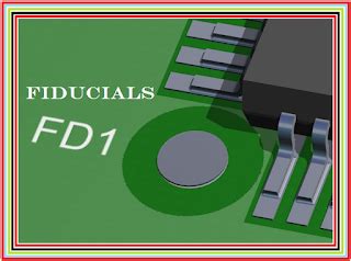
Fiducials, derived from the Latin word “fiducia” meaning “trust” or “confidence,” serve as trusted reference markers that guide the assembly process. They are typically round copper pads solder-masked on the outer layers of a PCB, contrasting with the board color for easy optical recognition.
The Importance of PCB Fiducials
Ensuring Accurate Component Placement
The primary purpose of PCB fiducials is to guarantee the accurate positioning of components during the automated assembly process. High-precision pick-and-place machines use fiducials as reference points to calibrate their coordinates and place components on the PCB with tight tolerances.
Misaligned or incorrectly placed components can lead to various issues, such as:
– Poor soldering
– Shorts or open circuits
– Mechanical stress on components
– Reduced reliability and performance
By utilizing fiducials, manufacturers can minimize placement errors and enhance the overall quality of the assembLED PCB.
Facilitating Automated Optical Inspection
Fiducials also play a crucial role in automated optical inspection (AOI) systems, which verify the correctness of component placement and soldering after the assembly process. AOI machines use fiducials as reference points to align their cameras and perform accurate inspections.
Without fiducials, AOI systems may struggle to consistently locate and inspect components, leading to potential quality control issues and increased manual inspection requirements.
Enabling Efficient Panelization
PCB Panelization involves grouping multiple identical or different PCB Designs onto a single panel for efficient manufacturing. Fiducials are essential for panelization, as they allow the assembly equipment to identify and process individual boards within the panel accurately.
Panelization fiducials, also known as global fiducials, are placed on the edges of the panel and serve as common reference points for all boards in the panel. These fiducials ensure proper alignment and orientation of the panel during the assembly process.

Types of PCB Fiducials
There are two main types of fiducials used in PCB manufacturing:
-
Global Fiducials (Panel Fiducials): These fiducials are placed on the edges of a PCB panel and serve as reference points for the entire panel. They are used to align the panel correctly in the assembly machines and ensure accurate placement of components on each individual board within the panel.
-
Local Fiducials (Board Fiducials): Local fiducials are placed on each individual PCB within a panel. They provide reference points for the specific board and are used by pick-and-place machines and AOI systems to accurately place and inspect components on that particular board.
Additionally, there are some specialized fiducials:
-
Stencil Fiducials: Used to align solder paste stencils during the solder paste application process.
-
Fiducial Marks for Connector Placement: Assist in accurately placing connectors and other mechanically critical components.

Fiducial Design Guidelines
To ensure optimal performance and compatibility with assembly equipment, follow these guidelines when designing fiducials:
Fiducial Size and Shape
- Fiducials should be circular, with a diameter between 1.0 mm and 2.0 mm.
- The most common sizes are 1.5 mm and 1.0 mm, but the exact size may depend on the specific requirements of the assembly equipment.
- Avoid using square or rectangular fiducials, as they can be challenging for vision systems to locate accurately.
Fiducial Copper Diameter
- The copper diameter of the fiducial should be between 1.0 mm and 2.0 mm.
- A copper diameter of 1.5 mm is most commonly used.
Soldermask Opening
- The soldermask opening should be slightly larger than the copper diameter to ensure visibility.
- A typical soldermask opening is 2.0 mm for a 1.5 mm copper diameter.
Placement and Clearance
- Place fiducials near the corners of the PCB, preferably within 5-10 mm from the edges.
- Ensure a minimum clearance of 3-5 mm between fiducials and other components or features on the PCB.
- Avoid placing fiducials under components or in areas with high component density.
Quantity and Distribution
- Use a minimum of 3 fiducials per PCB, positioned in a non-collinear pattern (e.g., forming a triangle).
- For larger PCBs or panels, use additional fiducials to ensure accurate alignment across the entire surface.
- Distribute fiducials evenly across the PCB or panel to minimize localized distortion effects.
Here’s a table summarizing the key fiducial design parameters:
| Parameter | Recommendation |
|---|---|
| Shape | Circular |
| Size (Diameter) | 1.0 mm – 2.0 mm (1.5 mm most common) |
| Copper Diameter | 1.0 mm – 2.0 mm (1.5 mm most common) |
| Soldermask Opening | Slightly larger than copper diameter (2.0 mm for 1.5 mm copper) |
| Placement | Near corners, 5-10 mm from edges |
| Clearance | 3-5 mm from other components and features |
| Quantity | Minimum 3 per PCB, non-collinear |

Best Practices for Using Fiducials
To maximize the effectiveness of fiducials in your PCB Assembly process, consider the following best practices:
-
Collaborate with your assembly partner: Consult with your PCB assembly provider early in the design process to ensure that your fiducial design meets their equipment requirements and guidelines.
-
Maintain consistency: Use consistent fiducial sizes, shapes, and placement across all your PCB designs to streamline the assembly setup process and minimize the need for machine adjustments.
-
Ensure adequate contrast: Fiducials should be easily distinguishable from the PCB background color. Typically, bare copper fiducials on a green soldermask provide sufficient contrast for most vision systems.
-
Avoid Solder Mask or silkscreen on fiducials: Keep fiducials free of any solder mask or silkscreen to maintain their visibility and ensure accurate detection by vision systems.
-
Consider panelization requirements: When panelizing PCBs, ensure that global fiducials are placed on the panel edges and local fiducials are placed on each individual board within the panel.
-
Verify fiducial compatibility: Before finalizing your design, verify that your fiducial placement and design are compatible with the specific assembly equipment and processes used by your manufacturer.
-
Keep fiducials clear of obstacles: Ensure that fiducials are not obstructed by tall components, connectors, or other features that may interfere with the vision system’s line of sight.
Troubleshooting Fiducial Issues
Despite careful design and adherence to best practices, issues related to fiducials can still arise during the assembly process. Here are some common problems and potential solutions:
- Fiducials not detected by vision system:
- Check if the fiducial size and shape meet the equipment requirements.
- Verify that the soldermask opening is large enough to provide adequate contrast.
- Ensure that the fiducials are free of solder mask, silkscreen, or other obstructions.
-
Confirm that the fiducials have sufficient clearance from nearby components.
-
Inconsistent component placement:
- Verify that the fiducials are correctly designed and placed on the PCB.
- Check if the fiducials are evenly distributed and not collinear.
- Ensure that the PCB is correctly aligned and secured in the assembly machine.
-
Recalibrate the pick-and-place machine using the fiducials as reference points.
-
Inaccurate alignment during panelization:
- Confirm that global fiducials are correctly placed on the panel edges.
- Verify that local fiducials are present on each individual board within the panel.
- Check if the fiducial design is consistent across all boards in the panel.
- Ensure that the panel is correctly loaded and aligned in the assembly machine.
If issues persist, consult with your PCB assembly provider for further assistance and guidance specific to their equipment and processes.
Frequently Asked Questions (FAQ)
-
What is the purpose of a PCB fiducial?
PCB fiducials serve as reference points for pick-and-place machines and automated optical inspection systems to accurately place and inspect components on the PCB during the assembly process. -
How many fiducials should be used on a PCB?
A minimum of three fiducials should be used on a PCB, positioned in a non-collinear pattern. Larger PCBs or panels may require additional fiducials for improved accuracy. -
What size should PCB fiducials be?
Fiducials should be circular, with a copper diameter between 1.0 mm and 2.0 mm. The most common sizes are 1.5 mm and 1.0 mm, but the exact size may depend on the specific requirements of the assembly equipment. -
Can fiducials be covered with solder mask or silkscreen?
No, fiducials should be kept free of solder mask and silkscreen to maintain their visibility and ensure accurate detection by vision systems. -
What should I do if my assembly partner is having issues with my fiducials?
Collaborate with your assembly partner to identify the specific issues they are encountering. Review your fiducial design and placement to ensure they meet the equipment requirements and guidelines. If necessary, make adjustments to your design and resend the updated files for assembly.
Conclusion
PCB fiducials play a critical role in ensuring accurate component placement and inspection during the PCB assembly process. By understanding the importance of fiducials, following design guidelines, and adhering to best practices, you can enhance the quality and reliability of your PCB assembly.
Remember to collaborate with your assembly partner, maintain consistency in your fiducial design, and verify compatibility with their specific equipment and processes. If issues arise, work closely with your manufacturer to troubleshoot and find appropriate solutions.
By effectively implementing PCB fiducials in your designs, you can streamline the assembly process, reduce errors, and ultimately achieve higher-quality PCB assemblies.
No responses yet