What is Soldermask?
Soldermask is a thin, protective coating that is applied to the copper traces of a PCB. It is typically made of a photosensitive polymer that hardens when exposed to light. The primary functions of soldermask are:
- Protection: Soldermask protects the copper traces from oxidation, corrosion, and mechanical damage.
- Insulation: It provides electrical insulation between adjacent copper traces, preventing short circuits and improving the reliability of the PCB.
- Solder control: Soldermask defines the areas where solder can be applied, preventing Solder Bridges and ensuring proper solder joint formation.
- Aesthetics: Soldermask is available in various colors, allowing for improved visual appearance and branding of the PCB.
Methods of Exposing Soldermask
There are several methods used to expose the soldermask during PCB production. The choice of method depends on factors such as the desired resolution, throughput, and cost. The most common methods include:
1. Screen Printing
Screen printing is a traditional method of applying and exposing soldermask. It involves the use of a fine mesh screen with a stencil of the desired soldermask pattern. The soldermask is applied to the PCB through the screen using a squeegee, and then exposed to UV light to harden the polymer. The advantages of screen printing include:
- Low cost for small to medium production runs
- Flexibility in terms of soldermask thickness and color options
- Suitable for larger feature sizes (>100 μm)
However, screen printing has some limitations, such as:
- Lower resolution compared to other methods
- Potential for screen blockage and inconsistent application
- Slower throughput compared to other methods
2. Photolithography
Photolithography is a high-resolution method of exposing soldermask that involves the use of a photomask and UV light. The process begins with the application of a thin, uniform layer of photosensitive soldermask to the PCB. A photomask, which contains the desired soldermask pattern, is then placed on top of the soldermask. The assembly is exposed to UV light, which causes the exposed areas of the soldermask to harden. The unexposed areas are then removed using a developer solution, leaving behind the desired soldermask pattern. The advantages of photolithography include:
- High resolution (down to 50 μm or less)
- Excellent pattern definition and consistency
- Suitable for high-volume production
However, photolithography also has some drawbacks:
- Higher cost compared to screen printing
- Longer setup times and more complex process steps
- Requires a clean room environment to prevent contamination
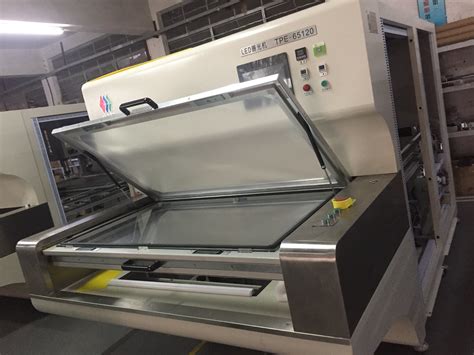
3. Direct Imaging
Direct imaging is a modern method of exposing soldermask that combines the advantages of screen printing and photolithography. In this process, the soldermask is applied to the PCB using a inkjet or aerosol printer, which deposits the soldermask directly onto the desired areas. The deposited soldermask is then immediately exposed to UV light using a high-resolution digital light processing (DLP) or laser imaging system. This eliminates the need for a physical photomask and allows for quick and easy changes to the soldermask pattern. The advantages of direct imaging include:
- High resolution (down to 25 μm or less)
- Excellent pattern definition and consistency
- Fast setup times and high throughput
- Reduced waste and lower cost compared to photolithography
However, direct imaging also has some limitations:
- Higher initial equipment cost compared to screen printing and photolithography
- Requires specialized soldermask formulations and printing equipment
- May have limitations in terms of soldermask thickness and color options

Factors Affecting Soldermask Exposure
Several factors can influence the success of soldermask exposure, regardless of the method used. These include:
-
Soldermask formulation: The chemical composition of the soldermask, including the type of polymer, photoinitiator, and additives, can affect its exposure characteristics and final properties.
-
Exposure energy and time: The amount of UV light energy and exposure time must be carefully controlled to ensure proper hardening of the soldermask without causing overexposure or underexposure.
-
Alignment and registration: Proper alignment and registration between the soldermask pattern and the underlying copper traces is critical to ensure accurate feature definition and prevent soldermask encroachment.
-
Surface preparation: The PCB surface must be clean, dry, and free of contaminants to ensure good adhesion of the soldermask and prevent defects such as voids or delamination.
-
Post-exposure processing: After exposure, the soldermask must be properly developed, cured, and cleaned to achieve the desired final properties and appearance.

Table: Comparison of Soldermask Exposure Methods
| Method | Resolution | Throughput | Cost | Flexibility |
|---|---|---|---|---|
| Screen Printing | Low | Medium | Low | High |
| Photolithography | High | High | Medium | Medium |
| Direct Imaging | Very High | Very High | High | Low |

Frequently Asked Questions (FAQ)
-
What is the recommended soldermask thickness for PCBs?
The typical soldermask thickness for PCBs ranges from 0.5 to 2.0 mils (12.7 to 50.8 μm). The exact thickness depends on the specific application, soldermask material, and exposure method used. -
Can soldermask be applied and exposed on both sides of the PCB?
Yes, soldermask can be applied and exposed on both sides of the PCB. This is commonly done for double-sided and multi-layer PCBs to provide protection and insulation on all exposed copper surfaces. -
What are the most common soldermask colors?
The most common soldermask colors are green, blue, red, and black. Other colors, such as white, yellow, and purple, are also available for specialized applications or visual effects. -
How does soldermask affect the electrical properties of the PCB?
Soldermask has a relatively minor effect on the electrical properties of the PCB. It can slightly increase the dielectric constant and dissipation factor of the PCB substrate, but these effects are typically negligible for most applications. -
What are the environmental and safety considerations for soldermask exposure?
Soldermask exposure involves the use of UV light and chemical developers, which can pose safety and environmental risks if not properly controlled. Proper ventilation, personal protective equipment (PPE), and waste disposal procedures must be followed to ensure the safety of workers and compliance with environmental regulations.
In conclusion, exposing the soldermask is a critical step in the PCB manufacturing process that requires careful selection of the exposure method, control of process parameters, and consideration of various factors affecting the final quality and performance of the soldermask. By understanding the different methods and their advantages and limitations, PCB Manufacturers can optimize their soldermask exposure process to achieve the desired results and meet the specific requirements of their customers.
No responses yet