Understanding Solder Escape and Its Causes
Solder escape, also known as solder wicking, is a common issue encountered during the reflow soldering process in PCB Assembly. It occurs when molten solder flows away from its intended location, such as component leads or pads, and spreads onto undesired areas of the printed circuit board. This phenomenon can lead to various problems, including short circuits, poor electrical connections, and aesthetic defects.
Several factors contribute to the occurrence of solder escape during reflow:
- Improper Solder Paste application
- Inadequate stencil design
- Incorrect reflow profile
- Poor PCB design and layout
- Contamination on the PCB surface
The Role of Solder Paste in Solder Escape
Solder paste plays a crucial role in the reflow soldering process. It is a mixture of tiny solder particles suspended in a flux medium. The consistency and composition of the solder paste can significantly impact its performance during reflow.
| Solder Paste Property | Effect on Solder Escape |
|---|---|
| Viscosity | High viscosity paste reduces the likelihood of solder escape |
| Particle Size | Smaller particles are more prone to solder escape |
| Flux Activity | Highly active flux can promote solder escape |
To minimize the risk of solder escape, it is essential to select a solder paste with the appropriate properties for your specific application. Consult with your solder paste supplier to determine the optimal formulation.
Stencil Design Considerations
The stencil is responsible for depositing the solder paste onto the PCB pads. A well-designed stencil ensures precise and consistent solder paste application. Consider the following factors when designing your stencil:
- Aperture Size and Shape
- Ensure aperture dimensions match the pad size and shape
- Avoid overly large or small apertures
- Stencil Thickness
- Thicker stencils deposit more solder paste, reducing the risk of solder escape
- Typical stencil thicknesses range from 0.100mm to 0.150mm
- Aperture Wall Geometry
- Tapered aperture walls facilitate solder paste release
- Straight walls may cause paste retention and increase the risk of solder escape
| Stencil Thickness (mm) | Recommended Aperture Size (mm) |
|---|---|
| 0.100 | 0.375 – 0.425 |
| 0.125 | 0.425 – 0.475 |
| 0.150 | 0.475 – 0.525 |
Note: The above recommendations are general guidelines. Actual aperture sizes may vary based on specific component requirements and PCB design.
Optimizing the Reflow Profile
The reflow profile defines the temperature and duration of the various stages in the reflow soldering process. An optimized reflow profile is essential for achieving good solder joint quality and minimizing solder escape. Consider the following tips when developing your reflow profile:
- Preheat Stage
- Gradually raise the temperature to activate the flux and evaporate solvents
- Avoid rapid temperature ramps that can cause solder paste slumping
- Soak Stage
- Maintain a stable temperature to allow the flux to clean the PCB and component surfaces
- Excessive soak time can lead to flux exhaustion and increased solder escape risk
- Reflow Stage
- Reach the peak temperature quickly to minimize the time molten solder is exposed
- Peak temperature should be high enough to fully melt the solder but not cause damage to components
- Cooling Stage
- Controlled cooling prevents thermal shock and ensures proper solder joint formation
- Rapid cooling can cause solder escape due to sudden contraction
| Reflow Profile Stage | Typical Temperature Range (°C) | Duration (seconds) |
|---|---|---|
| Preheat | 25 – 150 | 60 – 120 |
| Soak | 150 – 180 | 60 – 120 |
| Reflow | 220 – 250 | 30 – 90 |
| Cooling | 250 – 25 | 60 – 120 |
Note: The above values are general guidelines. Actual temperature ranges and durations may vary based on the specific solder paste and PCB assembly requirements.

PCB Design and Layout Tips
Proper PCB design and layout practices can significantly reduce the occurrence of solder escape. Consider the following tips:
- Pad Design
- Ensure pads are appropriately sized for the component leads
- Avoid excessively large or small pads
- Use solder thieves to control solder flow and prevent escape
- Trace Spacing
- Maintain adequate spacing between traces to prevent solder bridging
- Follow the minimum spacing guidelines provided by your PCB Manufacturer
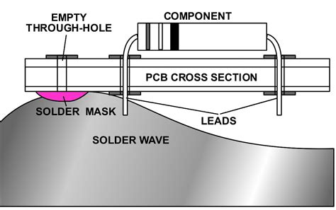
- Solder Mask Design
- Apply solder mask over areas where solder escape is undesirable
- Ensure proper solder mask alignment and registration
- Component Placement
- Arrange components to minimize the risk of solder escape
- Avoid placing components too close to the PCB edge or other critical areas
| Component Pitch (mm) | Minimum Pad Size (mm) | Minimum Trace Spacing (mm) |
|---|---|---|
| 0.5 | 0.25 x 0.25 | 0.15 |
| 0.8 | 0.40 x 0.40 | 0.20 |
| 1.27 | 0.60 x 0.60 | 0.30 |
Note: The above values are general guidelines. Actual pad sizes and trace spacing may vary based on the specific component and PCB manufacturing capabilities.

Contamination Control
Contamination on the PCB surface can interfere with the solder wetting process and contribute to solder escape. Common contaminants include:
- Flux residues
- Fingerprints and oils
- Dust and debris
- Oxidation
To minimize contamination:
- Handle PCBs with gloves to avoid fingerprints and oils
- Clean the PCB surface with isopropyl alcohol before solder paste application
- Store PCBs in a clean, dry environment
- Use a Nitrogen Reflow environment to reduce oxidation

Frequently Asked Questions (FAQ)
1. What is solder escape, and why is it a concern?
Solder escape, also known as solder wicking, occurs when molten solder flows away from its intended location and spreads onto undesired areas of the PCB. It can cause short circuits, poor electrical connections, and aesthetic defects, compromising the reliability and functionality of the PCB assembly.
2. How can I select the right solder paste to prevent solder escape?
When selecting a solder paste, consider factors such as viscosity, particle size, and flux activity. A high-viscosity paste with larger particles and moderate flux activity is generally less prone to solder escape. Consult with your solder paste supplier to determine the optimal formulation for your specific application.
3. What role does the stencil play in preventing solder escape?
The stencil is responsible for depositing the solder paste onto the PCB pads. A well-designed stencil with appropriate aperture sizes, thickness, and wall geometry ensures precise and consistent solder paste application, reducing the risk of solder escape.
4. How can I optimize my reflow profile to minimize solder escape?
An optimized reflow profile should have a gradual preheat stage, a stable soak stage, a quick reflow stage, and a controlled cooling stage. Avoid rapid temperature changes and excessive time in the molten state to minimize the risk of solder escape.
5. What PCB design and layout practices can help prevent solder escape?
Proper pad design, adequate trace spacing, effective solder mask application, and strategic component placement can all contribute to reducing the occurrence of solder escape. Follow the guidelines provided by your PCB manufacturer and consider using solder thieves to control solder flow.
Conclusion
Preventing solder escape during the reflow soldering process is essential for achieving high-quality and reliable PCB assemblies. By understanding the causes of solder escape and implementing best practices in solder paste selection, stencil design, reflow profile optimization, PCB design, and contamination control, you can significantly reduce the risk of solder escape and improve the overall success of your PCB assembly process.
Remember to consult with your suppliers, follow industry guidelines, and continuously monitor and optimize your process to achieve the best results. With the right knowledge and techniques, you can overcome the challenges of solder escape and produce consistently high-quality PCB assemblies.
No responses yet