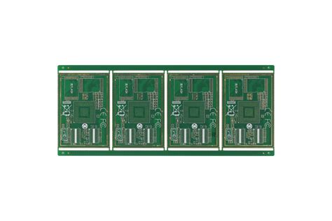
What are PCB Castellations?
PCB castellations are a type of edge connector consisting of plated semi-circular cut-outs or tabs along the edge of a printed circuit board (PCB). The term “castellation” comes from their resemblance to the battlement structures along the top of a castle wall. Castellations provide a simple, robust, and space-saving method for connecting PCBs together or to other components without requiring additional connectors.
Castellated holes are typically plated with copper, gold, or tin to form conductive pads that can be soldered to corresponding pads on another board or component. This creates an electrical and mechanical connection between the two parts.
Key features of PCB castellations:
- Semi-circular cut-outs or tabs along board edge
- Plated with conductive material to form connectable pads
- Provide board-to-board or board-to-component connections
- Eliminate need for separate connectors
- Enable compact, high-density designs
- Ideal for modular and plug-in systems
How are Castellations Formed?
The castellation process is performed during PCB fabrication, after the copper traces and other features have been etched but before the board is cut out from the production panel. There are two main methods for forming castellations:
Routing
Castellated holes can be formed by using a routing tool to cut semi-circular grooves along the edge of the board. The router bit follows the outline of each castellation, cutting through the copper and substrate. This leaves a series of half-circle cut-outs with the plated edges exposed.
Drilling
Alternatively, castellations can be created by drilling a series of overlapping holes along the board edge. The holes are drilled close enough together that they intersect, leaving a row of plated semi-circles. The remaining material between the holes is then routed away to separate the individual boards from the panel.
In both cases, the plating process ensures that the castellation edges are conductive and suitable for soldering. Additional Surface Finish, such as Gold plating, may be applied to protect the exposed copper and enhance solderability.

Advantages of Using Castellations
PCB castellations offer several benefits compared to other connection methods:
-
Space savings: Castellations eliminate the need for separate connectors, allowing for more compact designs. This is especially valuable in applications where board space is limited.
-
Simplified assembly: Connecting castellated boards is a straightforward process of aligning the pads and soldering them together. This can be done manually or using automated assembly equipment.
-
Modular design: Castellations enable modular architectures where multiple boards can be plugged together to form a larger system. This allows for flexibility, easy customization, and future upgrades.
-
High connection density: The small size and close spacing of castellations allow for a high number of connections along the board edge. This is useful for high-speed signals or applications requiring many interconnects.
-
Mechanical strength: Soldered castellations create a strong mechanical bond between boards, helping to hold them securely in place. The interlocking nature of the castellations adds rigidity to the assembly.
-
Cost-effective: By using the PCB itself as the connector, castellations can reduce overall system cost by eliminating the need for separate connectors and simplifying assembly.

Design Considerations for Castellations
When designing a PCB with castellations, there are several factors to consider:
Castellation Dimensions
The size and spacing of the castellations will depend on the specific application and the capabilities of the PCB Manufacturer. Common dimensions for castellation holes are:
| Dimension | Typical Value |
|---|---|
| Diameter | 0.8 – 1.2 mm |
| Spacing | 1.2 – 2.0 mm |
| Plating thickness | 25 – 50 μm |
Smaller castellations allow for higher density but may be more challenging to manufacture and assemble. It’s important to consult with the PCB fabricator to ensure the desired dimensions are feasible.
Pad Design
The pads on the mating board or component must be designed to match the layout of the castellations. The pad size should be slightly larger than the castellation diameter to allow for alignment tolerances and a reliable solder joint.
Pad shape is also a consideration. Round pads are common, but oblong or rectangular pads can provide additional surface area for soldering. Teardrops or filleted pads can help to strengthen the joint and reduce stress concentrations.
Plating and Surface Finish
The castellations should be plated with a conductive material to form a solderable surface. Copper is the most common base plating, often with additional layers of nickel and gold to protect the copper and improve solderability.
The thickness of the plating should be sufficient to ensure a reliable connection and withstand the soldering process. A minimum plating thickness of 25 μm is typical, but thicker plating may be specified for high-reliability applications.
Solder Mask
Solder mask is typically used to cover the PCB surface, except for the exposed pads and castellations. This helps to prevent solder bridging and short circuits.
The solder mask aperture should be sized to fully expose the castellation pad while providing some overlap onto the board surface. This overlap helps to anchor the solder mask and prevent it from lifting away during soldering.
Mechanical Support
In some cases, additional mechanical support may be needed to hold the castellated boards securely in place. This can be achieved through the use of fasteners, standoffs, or other hardware.
Designing interlocking features or tabs into the board outline can also help to align and secure the boards during assembly. These features should be carefully designed to avoid interfering with the electrical connections or causing undue stress on the castellations.

Assembly and Soldering of Castellations
Assembling castellated boards requires precise alignment and a controlled soldering process. The steps typically involve:
-
Align the castellations with the corresponding pads on the mating board or component. Visual alignment guides or mechanical features can aid in this process.
-
Hold the boards in place using fixturing or temporary adhesives. Ensure the castellations remain in contact with the pads.
-
Apply solder to the castellations, either through hand soldering, wave soldering, or Reflow Soldering. The choice of soldering method will depend on the specific application and production volume.
-
Inspect the solder joints for proper wetting, fillets, and absence of defects such as bridging or voids. X-ray inspection may be necessary for hidden joints.
-
Clean the assembly to remove any flux residue or contaminants.
Proper process control is essential to achieve reliable solder joints. This includes managing factors such as solder alloy composition, flux type, soldering temperature profile, and cleaning methods.
Common Applications of Castellations
PCB castellations are used in a wide range of electronic applications, including:
- Modular systems and plug-in cards
- High-density interconnects
- Board-to-board stacking
- Mezzanine boards and daughtercards
- Edge connector interfaces
- Sensor modules and probe assemblies
- LED lighting arrays
Castellations are particularly well-suited for applications requiring high interconnect density, modular design, or limited board space.
Frequently Asked Questions (FAQ)
1. What is the difference between castellations and edge connectors?
Castellations are a type of edge connector where the connections are formed directly on the PCB edge. Traditional edge connectors use separate metal contacts that are attached to the PCB. Castellations offer a more integrated and space-saving solution.
2. Can castellations be used for high-speed signals?
Yes, castellations can be used for high-speed signals. The small size and close spacing of castellations allow for short, low-impedance connections that are suitable for high-frequency applications. However, careful design and layout practices must be followed to ensure signal integrity.
3. Are castellations suitable for high-power applications?
Castellations can be used in high-power applications, but the power handling capability will be limited by the size and number of castellations. Larger castellations or multiple rows of castellations may be needed to carry higher currents. Thermal management and current density limits must also be considered.
4. How do castellations affect PCB manufacturing cost?
Adding castellations to a PCB design may increase manufacturing cost due to the additional processing steps required. The castellation forming process, whether routing or drilling, adds complexity to the fabrication process. However, the overall system cost may be reduced by eliminating the need for separate connectors and simplifying assembly.
5. Can castellations be repaired if damaged?
Damaged castellations can be difficult to repair, especially if the plating is compromised. In some cases, careful hand soldering may be able to bridge a damaged castellation. However, if the damage is severe or the connection is critical, the best solution may be to replace the entire board.
Conclusion
PCB castellations offer a compact, reliable, and cost-effective method for connecting printed circuit boards. By eliminating the need for separate connectors, castellations enable high-density interconnects and modular designs. Proper design and manufacturing processes are essential to ensure reliable electrical and mechanical performance. As electronic systems continue to miniaturize and modularize, castellations will play an increasingly important role in PCB design and assembly.
No responses yet