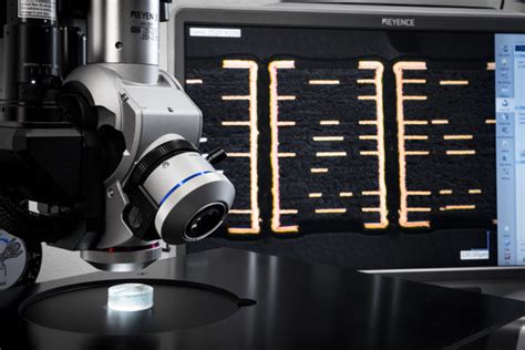
Why is Via Filling Important?
Via filling plays a crucial role in the functionality and reliability of PCBs. Here are some key reasons why via filling is important:
-
Electrical Conductivity: By filling the vias with a conductive material, electrical signals can pass through the holes and connect different layers of the PCB. This ensures proper connectivity and signal integrity throughout the board.
-
Mechanical Strength: Filled vias provide additional mechanical strength to the PCB. The filling material helps to reinforce the structure of the board, making it more resistant to stress and vibration.
-
Thermal Management: In high-power applications, via filling can help dissipate heat from one layer to another. The filling material acts as a thermal conduit, allowing heat to transfer more efficiently and preventing localized hot spots on the PCB.
-
Signal Integrity: Filled vias can minimize signal distortion and improve signal integrity. By providing a solid, continuous path for electrical signals, filled vias reduce the risk of signal reflections and crosstalk.
-
High-Density Interconnects: Via filling enables the creation of high-density interconnects (HDI) in PCBs. With the ability to fill small-diameter vias, designers can pack more components and connections into a smaller board area, facilitating the development of compact and complex electronic devices.
Via Filling Process
The via filling process typically involves several steps. Here is a general overview of the process:
-
Drilling: The first step is to drill the vias into the PCB using a computer-controlled drilling machine. The size and location of the vias are determined by the PCB design.
-
Desmear: After drilling, the vias undergo a desmear process to remove any residual debris and prepare the hole walls for plating. This step ensures good adhesion between the filling material and the via walls.
-
Electroless Copper Plating: An electroless copper plating process is used to deposit a thin layer of copper onto the walls of the vias. This layer acts as a seed layer for the subsequent electrolytic plating process.
-
Electrolytic Copper Plating: The PCB is then subjected to an electrolytic copper plating process, where a thicker layer of copper is deposited onto the via walls and the surface of the PCB. This step helps to build up the copper thickness to the desired level.
-
Filling: Once the vias are plated, they are filled with a conductive material. The most common filling material is copper, which is applied using a specialized via filling machine. The machine forces the filling material into the vias under pressure, ensuring complete and void-free filling.
-
Planarization: After filling, the PCB undergoes a planarization process to remove any excess filling material from the surface of the board. This step ensures a flat and even surface for subsequent processing steps.
-
Final Plating: Finally, the PCB may undergo additional plating processes, such as solder mask application and Surface Finish, to protect the copper and prepare the board for component assembly.

Types of Via Filling
There are several types of via filling techniques used in PCB manufacturing. The choice of technique depends on factors such as the via size, aspect ratio, and the specific requirements of the application. Here are some common types of via filling:
-
Copper Filling: Copper is the most widely used material for via filling. It offers excellent electrical conductivity, thermal conductivity, and mechanical strength. Copper filling can be achieved through electroplating or paste filling processes.
-
Conductive Paste Filling: Conductive paste, also known as via fill paste, is a popular alternative to copper filling. The paste is a mixture of conductive particles (e.g., silver, copper, or gold) suspended in a polymer matrix. It is applied to the vias using a screen printing or stencil printing process and then cured to form a solid, conductive fill.
-
Conductive Ink Filling: Conductive ink filling involves using a specialized ink that contains conductive particles. The ink is dispensed into the vias using an ink-jet printing process and then cured to form a conductive fill. This method is suitable for small-diameter vias and high-density applications.
-
Resin Filling: Resin filling is a non-conductive via filling technique. It involves filling the vias with a non-conductive epoxy resin. While it does not provide electrical conductivity, resin filling can improve the mechanical strength and thermal stability of the PCB.

Challenges in Via Filling
Via filling is a complex process that comes with its own set of challenges. Some of the common challenges encountered in via filling include:
-
Void Formation: One of the main challenges in via filling is the formation of voids or air pockets within the filled vias. Voids can occur due to insufficient filling, poor wetting of the via walls, or improper curing of the filling material. Voids can compromise the electrical and mechanical integrity of the PCB.
-
Aspect Ratio: The aspect ratio of a via refers to the ratio of its depth to its diameter. High aspect ratio vias (deep and narrow) are more challenging to fill completely and uniformly compared to low aspect ratio vias. Special techniques and equipment may be required to achieve reliable filling in high aspect ratio vias.
-
Material Compatibility: The choice of filling material must be compatible with the PCB substrate and the plating processes used. Incompatible materials can lead to poor adhesion, delamination, or other reliability issues.
-
Process Control: Via filling involves multiple process steps, each of which must be carefully controlled to ensure consistent and reliable results. Factors such as temperature, pressure, and fill time must be optimized to achieve the desired filling quality.
-
Cost: Via filling can add significant cost to the PCB manufacturing process, especially for high-volume production. The cost of equipment, materials, and process time must be carefully considered when implementing via filling in a PCB design.

Advancements in Via Filling Technology
As the demand for high-density interconnects and miniaturization continues to grow, via filling technology has evolved to meet these challenges. Here are some recent advancements in via filling technology:
-
Selective Via Filling: Selective via filling allows for the filling of specific vias on a PCB while leaving others unfilled. This technique enables designers to optimize the via filling process based on the specific requirements of different parts of the board, reducing costs and improving efficiency.
-
Laser Via Filling: Laser via filling is an emerging technology that uses a laser to melt and fill the vias with a conductive material. This method offers high precision, speed, and the ability to fill vias with a wide range of materials, including copper, gold, and silver.
-
3D Via Filling: 3D via filling is a technique used in the fabrication of three-dimensional (3D) PCBs. It involves filling the vias that connect different layers of a 3D PCB stack, enabling vertical interconnects between the layers. 3D via filling is crucial for the development of advanced packaging solutions, such as system-in-package (SiP) and package-on-package (PoP) designs.
-
Conductive Polymer Filling: Conductive polymers, such as intrinsically conductive polymers (ICPs), are being explored as an alternative to traditional metal filling materials. These polymers offer advantages such as lower cost, lighter weight, and the ability to fill complex via geometries.
FAQ
-
Q: What is the difference between Blind Vias and buried vias?
A: Blind vias are vias that start from one surface of the PCB and terminate at an inner layer, while buried vias are vias that connect two or more inner layers without reaching either surface of the PCB. -
Q: Can via filling improve the thermal management of a PCB?
A: Yes, via filling can help with thermal management by providing a path for heat to dissipate from one layer to another. Filled vias act as Thermal Vias, allowing heat to transfer more efficiently and preventing localized hot spots on the PCB. -
Q: What is the most common material used for via filling?
A: Copper is the most common material used for via filling. It offers excellent electrical conductivity, thermal conductivity, and mechanical strength. Copper filling can be achieved through electroplating or paste filling processes. -
Q: How does via filling affect the cost of PCB manufacturing?
A: Via filling can add significant cost to the PCB manufacturing process, especially for high-volume production. The cost of equipment, materials, and process time must be carefully considered when implementing via filling in a PCB design. However, the benefits of via filling, such as improved reliability and performance, often outweigh the additional cost. -
Q: Can via filling be used in flexible PCBs?
A: Yes, via filling can be used in flexible PCBs. However, the choice of filling material and the filling process must be carefully considered to ensure compatibility with the flexible substrate and to maintain the flexibility of the PCB. Conductive polymers and conductive inks are often used for via filling in flexible PCBs.
Conclusion
Via filling is a critical process in the manufacturing of printed circuit boards, enabling reliable and high-density interconnects in modern electronic devices. By filling the vias with a conductive material, designers can improve the electrical conductivity, mechanical strength, thermal management, and signal integrity of PCBs.
The via filling process involves several steps, including drilling, desmear, plating, filling, planarization, and final plating. Different types of via filling techniques, such as copper filling, conductive paste filling, and conductive ink filling, are used depending on the specific requirements of the application.
While via filling presents challenges such as void formation, aspect ratio limitations, material compatibility, process control, and cost, advancements in technology are addressing these issues. Selective via filling, laser via filling, 3D via filling, and conductive polymer filling are some of the emerging technologies that are pushing the boundaries of via filling capabilities.
As electronic devices continue to become more complex and compact, via filling will remain a crucial aspect of PCB manufacturing. By understanding the importance, process, challenges, and advancements in via filling technology, designers and manufacturers can make informed decisions to optimize the performance and reliability of their PCBs.
| Via Filling Technique | Description | Advantages | Disadvantages |
|---|---|---|---|
| Copper Filling | Filling vias with copper through electroplating or paste | – Excellent electrical and thermal conductivity – High mechanical strength |
– Higher cost compared to other techniques – Challenging for high aspect ratio vias |
| Conductive Paste Filling | Filling vias with a paste containing conductive particles | – Lower cost compared to copper filling – Suitable for small vias |
– Lower conductivity compared to copper – Requires curing process |
| Conductive Ink Filling | Filling vias with a conductive ink using ink-jet printing | – Suitable for small-diameter vias and high-density applications – Faster process compared to paste filling |
– Limited choice of conductive materials – Requires specialized equipment |
| Resin Filling | Filling vias with a non-conductive epoxy resin | – Improves mechanical strength and thermal stability – Lower cost compared to conductive filling |
– Does not provide electrical conductivity – May require additional processing steps |
In summary, via filling is a vital process in PCB manufacturing that enables the creation of reliable and high-performance electronic devices. By carefully considering the various via filling techniques, challenges, and advancements, designers and manufacturers can optimize their PCB designs to meet the ever-increasing demands of the electronics industry.
No responses yet