Introduction to BGA Soldering
Ball Grid Array (BGA) is a popular surface-mount packaging used for integrated circuits. BGA packages provide more interconnection pins than can be put on a dual in-line or flat package. BGA soldering on printed circuit boards (PCBs) is a key process in surface mount technology (SMT) assembly.
Proper BGA soldering requires precise control of many factors including solder paste printing, component placement, reflow profile, and PCB design. Getting BGA soldering right is critical for manufacturing reliable, high-quality electronic assemblies.
This article covers 9 important ways to optimize the BGA soldering process in SMT assembly:
- Solder Paste Printing
- Component Placement
- Reflow Soldering Profile
- PCB Pad Design
- Solder Mask Design
- Via-in-Pad
- X-Ray Inspection
- Rework and Repair
- Process Control
1. Solder Paste Printing
Solder paste printing is the first step in the BGA soldering process. The right amount of solder paste must be deposited on each PCB pad. Too much paste can cause bridging, while too little may result in open joints.
Key factors in paste printing include:
- Stencil thickness
- Aperture size and shape
- Paste type and viscosity
- Print speed and pressure
- Board support and gasketing
Stencil Design
The stencil is the most important tool in the solder paste printing process. Laser-cut stainless steel stencils with electro-polished apertures provide the best print definition and release characteristics.
Stencil thickness depends on the size of the BGA bump:
| Bump Diameter | Stencil Thickness |
|---|---|
| < 0.25 mm | 0.100-0.125 mm |
| 0.25-0.30 mm | 0.125-0.150 mm |
| 0.30-0.40 mm | 0.150-0.200 mm |
| > 0.40 mm | 0.200-0.250 mm |
Aperture size is typically 80-90% of the pad size. The aperture walls should be tapered 5° to facilitate paste release.
Solder Paste
Solder paste is a homogeneous mixture of tiny solder spheres, flux, solvents, and modifiers. The metal content is usually 88-90% by weight.
No-clean, lead-free solder pastes are most common. SAC305 and SAC405 alloys provide a good balance of processability, reliability, and cost. The solder particle size should be appropriate for the pitch of the BGA:
| Pitch | Solder Powder Size |
|---|---|
| ≥ 1.27 mm | Type 3 (-325/+500 mesh) |
| 1.0-1.27 mm | Type 4 (-400/+635 mesh) |
| 0.8-1.0 mm | Type 5 (-500/+635 mesh) |
| ≤ 0.8 mm | Type 6 (-635 mesh) |
Print Parameters
Optimum print parameters depend on the solder paste, stencil, and substrate. Key variables include squeegee speed, pressure, and attack angle.
Typical print parameters:
– Print speed: 20-150 mm/sec
– Pressure: 0.18-0.27 N/mm of blade length
– Attack angle: 45-60°
Understencil cleaning at regular intervals is important to prevent paste bleeding and bridging. A solvent with at least 75% isopropyl alcohol is recommended.

2. Component Placement
Precise placement is critical for BGA soldering. The package outline should be centered on the paste deposit. Placement pressure should be sufficient to ensure paste contact but not so high as to cause smearing.
Typical placement parameters:
– Placement pressure: 1.5-4.0 N
– Placement speed: 10-50 mm/sec
– Placement accuracy: ±50 μm
Vision systems are used to verify paste alignment, component position, and package orientation before and after placement. Fiducials on the PCB and package facilitate accurate alignment.

3. Reflow Soldering
Reflow soldering melts and coalesces the solder particles to form a metallurgical bond between the package and PCB pads. The reflow profile must be carefully optimized and controlled to ensure complete melting and wetting of the solder joint.
Key stages of the reflow profile:
1. Preheat: Activates fluxes and evaporates solvents
2. Thermal soak: Minimizes thermal gradients
3. Reflow: Melts and wets the solder
4. Cooling: Solidifies the solder joint
Reflow profile parameters depend on the solder paste, substrate, and component thermal mass. Typical values:
| Stage | Temp (°C) | Time (sec) | Ramp Rate (°C/sec) |
|---|---|---|---|
| Preheat | 150-180 | 60-120 | 0.5-2 |
| Soak | 180-200 | 60-120 | 0.5-1 |
| Reflow | 235-250 | 30-90 | 1-3 |
| Cooling | < 180 | – | -2 to -6 |
The peak temperature should be 15-20°C above the solder liquidus. Time above liquidus should be 30-90 seconds. Cooling rate should be controlled to avoid component and PCB Warpage.
Thermocouples and profiling software are used to measure and optimize the reflow profile for each product. Regular oven maintenance and calibration are important for process consistency.

4. PCB Pad Design
Proper pad design is essential for robust BGA solder joints. The pad size and shape influence the amount of solder deposited and the final joint geometry.
Typical pad dimensions for lead-free BGAs:
| Bump Diameter | Pad Diameter | Pad Spacing |
|---|---|---|
| 0.25 mm | 0.30-0.35 mm | 0.65-0.75 mm |
| 0.30 mm | 0.35-0.40 mm | 0.75-0.80 mm |
| 0.40 mm | 0.45-0.55 mm | 0.80-1.00 mm |
| 0.50 mm | 0.55-0.65 mm | 1.00-1.27 mm |
Solder mask-defined (SMD) pads are most common. The mask opening is 50-100 μm larger than the copper pad. Copper-defined pads may be used for fine-pitch BGAs.
Non-solder mask defined (NSMD) pads provide better control of the solder joint volume and shape. The copper pad is larger than the mask opening, allowing solder to wet along the pad sidewall.
5. Solder Mask Design
Solder mask around BGA pads should be at least 1.5x the pad diameter to allow outgassing during reflow. Teardrop-shaped mask openings can reduce stress concentrations.
Via fanout and escape routing must be carefully designed to avoid solder wicking. Solder mask dams at least 100 μm wide should be used to prevent bridging between pads and traces.
Liquid photoimageable (LPI) solder masks are preferred for BGAs. The mask should be color-contrasted with the substrate for easy inspection.
6. Via-in-Pad
Vias in BGA pads (VIP) are often used to maximize board space utilization. However, special design and process considerations are required.
VIP parameters:
– Via diameter: 0.15-0.30 mm
– Via Fill: Conductive via fill is preferred to plugging
– Via catch pad: Equal to or smaller than the BGA pad
– Filling process: Screen printing, stencil printing, or via shooting
The via fill must be planar with the pad surface to avoid impacting solder paste printing and joint formation. Inadequate or non-uniform fill can cause voids and compromised joint reliability.
X-ray inspection is recommended to verify via fill quality before assembly.
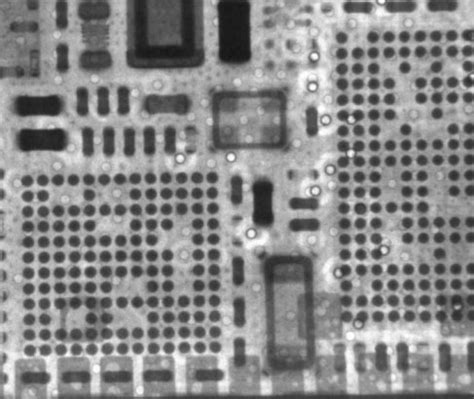
7. X-Ray Inspection
X-ray is the only non-destructive method to inspect BGA solder joints after reflow. Automated X-ray inspection (AXI) systems are commonly used for inline monitoring of joint quality.
AXI systems use oblique views and tomosynthesis to detect defects such as:
– Voids
– Bridging
– Opens
– Head-in-pillow
– Insufficient reflow
The head-in-pillow (HIP) defect is unique to BGAs. It occurs when the package and PCB pads are not properly wetted, resulting in an open circuit. HIP defects are difficult to detect by optical inspection.
3D computed tomography (CT) X-ray is sometimes used for failure analysis and process characterization. CT allows virtual cross-sectioning and measurement of individual solder joints.
8. Rework and Repair
BGA Rework involves removing and replacing defective components. It is a delicate and skill-intensive process.
Key steps in BGA rework:
1. Defect detection: X-ray inspection
2. Site preparation: Remove residual solder
3. Reballing: Apply new solder balls
4. Placement: Align and place new component
5. Reflow: Selective heating of component and pads
6. Inspection: X-ray verification of joint quality
Specialized BGA rework stations with vision alignment and localized heating are used to avoid damaging neighboring components. The heating profile should be similar to the original reflow profile.
Solder paste or flux is used to aid wetting during component placement. A stencil may be used for paste deposition.
Reballing requires precise control of ball size and placement. Prefabricated reball preforms are available for common BGA pitches. For non-standard pitches, a reball stencil may be required.
X-ray inspection should be performed after rework to verify joint quality and absence of damage. Cross-sectioning may be used for process validation.
9. Process Control
Robust BGA assembly requires continuous process monitoring and control. Statistical process control (SPC) methods are used to detect and correct variations before they result in defects.
Key process parameters to monitor:
– Solder paste viscosity and tackiness
– Paste volume and height
– Placement accuracy and pressure
– Reflow profile temperatures and times
– X-ray void percentage and size
Regular calibration and preventive maintenance of equipment is essential. Consumables such as solder paste and stencils should be stored and handled per manufacturer recommendations.
Traceability of materials, equipment, and processes enables rapid identification and correction of root causes when defects occur. A system for documenting and communicating best practices and lessons learned should be established.
Conclusion
BGA soldering is a critical process in SMT assembly. Achieving high yield and reliability requires careful design, material selection, process optimization, and control.
By following the 9 key principles outlined in this article, manufacturers can ensure consistent, high-quality BGA solder joints. However, continuous improvement and adaptation to new technologies and requirements is necessary to stay competitive in today’s dynamic electronics industry.
FAQ
1. What is the most common defect in BGA soldering?
The most common defect is the head-in-pillow (HIP) defect, where the solder balls on the component and PCB pads do not properly wet and coalesce. This results in an open circuit that is difficult to detect by optical inspection.
2. Can BGAs be reworked?
Yes, BGAs can be reworked using specialized equipment and techniques. The defective component is removed, the site prepared, and a new component placed and reflowed. X-ray inspection is used to verify rework quality.
3. What is the difference between SMD and NSMD BGA pads?
Solder mask-defined (SMD) pads have the solder mask opening smaller than the copper pad. Non-solder mask defined (NSMD) pads have the copper extending beyond the mask opening. NSMD provides better control of solder volume and joint shape.
4. How do you inspect BGA solder joints?
X-ray inspection is the only non-destructive method to verify BGA solder joint quality after reflow. Automated X-ray inspection (AXI) systems are used for inline monitoring, while 3D computed tomography (CT) is used for failure analysis.
5. What is the role of stencil design in BGA solder paste printing?
The stencil determines the volume and shape of solder paste deposited on the PCB pads. Stencil thickness, aperture size and shape, and material affect print quality and consistency. Laser-cut stainless steel stencils with electropolished apertures are preferred for BGAs.
No responses yet