What are PCB Vias?
PCB vias are conductive pathways used to electrically connect different layers of a printed circuit board (PCB). They allow signals and power to pass through the insulating material separating the layers, enabling more complex and compact circuit designs. Vias are essential components in multi-layer PCBs, as they facilitate interconnections between components on different layers.
Why are PCB Vias Important?
PCB vias play a crucial role in the design and functionality of multi-layer PCBs:
- Space Savings: Vias allow designers to create more compact PCB layouts by utilizing multiple layers, reducing the overall size of the board.
- Increased Connectivity: With vias, components on different layers can be interconnected, enabling more complex circuits and functionality.
- Improved Signal Integrity: Properly designed vias help maintain signal integrity by minimizing crosstalk and electromagnetic interference (EMI).
- Enhanced Thermal Management: Thermal vias can be used to dissipate heat from components, improving the overall thermal performance of the PCB.

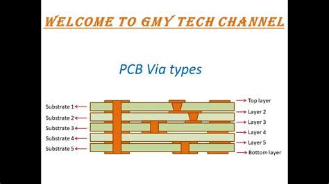
Types of PCB Vias
There are several types of PCB vias, each with their own characteristics and applications. Here are eight common types of vias:
1. Through-Hole Vias
Through-hole vias are the most basic type of via, created by drilling a hole through the entire thickness of the PCB and plating the inside of the hole with a conductive material. They provide a strong mechanical connection and are suitable for mounting through-hole components.
Advantages:
- Strong mechanical connection
- Suitable for through-hole components
- Easier to manufacture compared to other via types
Disadvantages:
- Consume more board space
- Limited routing flexibility
- Higher impedance compared to other via types
2. Blind Vias
Blind vias are partially drilled holes that start from one surface of the PCB and terminate at an inner layer, without passing through the entire board. They are used to connect an outer layer to one or more inner layers, providing more routing flexibility and saving board space.
Advantages:
- Save board space
- Increase routing flexibility
- Reduce layer count
Disadvantages:
- More expensive to manufacture
- Limited to connecting outer layers to inner layers
- Requires precise drilling control
3. Buried Vias
Buried vias are similar to blind vias, but they are located entirely within the inner layers of the PCB, without connecting to either surface. They are used to interconnect inner layers, further increasing routing flexibility and saving board space.
Advantages:
- Save even more board space
- Increase routing flexibility
- Reduce layer count
Disadvantages:
- Most expensive to manufacture
- Limited to connecting inner layers
- Requires precise drilling and lamination control
4. Microvias
Microvias are small, high-density vias with diameters typically less than 150 microns. They are created using laser drilling or photolithography techniques and are used in high-density interconnect (HDI) PCB designs to connect fine-pitch components and save board space.
Advantages:
- Enable high-density interconnects
- Save board space
- Suitable for fine-pitch components
Disadvantages:
- Expensive to manufacture
- Requires specialized equipment and processes
- Limited to connecting outer layers to inner layers
5. Stacked Vias
Stacked vias are a combination of blind or buried vias that are aligned vertically to connect multiple layers of a PCB. They are used to create interconnections between non-adjacent layers, further increasing routing flexibility and reducing layer count.
Advantages:
- Increase routing flexibility
- Reduce layer count
- Enable interconnections between non-adjacent layers
Disadvantages:
- More expensive to manufacture
- Requires precise alignment and drilling control
- May increase board thickness
6. Staggered Vias
Staggered vias are a pattern of vias arranged in an alternating or offset manner to reduce the size of the via pad and save board space. They are commonly used in high-density PCB designs where space is limited.
Advantages:
- Save board space
- Enable high-density routing
- Reduce via pad size
Disadvantages:
- More complex to design and manufacture
- May increase manufacturing costs
- Requires precise alignment and drilling control
7. Thermal Vias
Thermal vias are used to dissipate heat from components on the PCB by providing a low-resistance thermal path to a heatsink or ground plane. They are typically larger in diameter and placed in arrays around heat-generating components.
Advantages:
- Improve thermal management
- Prevent component overheating
- Enhance PCB reliability
Disadvantages:
- Consume board space
- May impact signal integrity if not properly designed
- Require careful placement and sizing
8. Via-in-Pad
Via-in-pad is a technique where a via is placed directly on a component pad, allowing for a more compact PCB layout and improved routing efficiency. This technique is commonly used in high-density designs and with ball grid array (BGA) components.
Advantages:
- Save board space
- Improve routing efficiency
- Enable high-density designs
Disadvantages:
- More complex to manufacture
- May require specialized equipment and processes
- Careful design and placement are necessary to avoid signal integrity issues

Designing with PCB Vias
When designing a PCB with vias, there are several considerations to keep in mind:
- Via Size: Choose the appropriate via size based on the current carrying requirements, manufacturing capabilities, and design constraints.
- Via Placement: Place vias strategically to minimize signal integrity issues, such as crosstalk and EMI, and to optimize routing efficiency.
- Via Spacing: Ensure adequate spacing between vias to maintain signal integrity and prevent manufacturing issues, such as drill breakout or shorts.
- Via Aspect Ratio: Consider the aspect ratio (depth to diameter) of the vias to ensure manufacturability and reliability.
- Via Filling: In some cases, vias may need to be filled with a non-conductive material to prevent solder wicking or to improve structural integrity.

PCB Via Manufacturing Processes
The manufacturing process for PCB vias depends on the type of via and the design requirements. Here are some common manufacturing processes:
- Drilling: Mechanical drilling is used to create through-hole vias and some blind vias. The process involves using a drill bit to create holes in the PCB.
- Laser Drilling: Laser drilling is used to create microvias and some blind vias. This process uses a focused laser beam to create small, precise holes in the PCB.
- Plating: After drilling, the vias are plated with a conductive material, such as copper, to create an electrical connection between layers.
- Lamination: For buried vias and some blind vias, the PCB Layers are laminated together before drilling to create the interconnections.
Frequently Asked Questions (FAQ)
- What is the difference between a through-hole via and a blind via?
-
A through-hole via passes through the entire thickness of the PCB, while a blind via starts from one surface and terminates at an inner layer without passing through the entire board.
-
What are microvias, and when are they used?
-
Microvias are small, high-density vias with diameters typically less than 150 microns. They are used in high-density interconnect (HDI) PCB designs to connect fine-pitch components and save board space.
-
How do thermal vias help with PCB thermal management?
-
Thermal vias provide a low-resistance thermal path from heat-generating components to a heatsink or ground plane, helping to dissipate heat and prevent component overheating.
-
What is via-in-pad, and what are its advantages?
-
Via-in-pad is a technique where a via is placed directly on a component pad, allowing for a more compact PCB layout and improved routing efficiency. It saves board space and enables high-density designs.
-
What are some key considerations when designing a PCB with vias?
- When designing a PCB with vias, consider factors such as via size, placement, spacing, aspect ratio, and filling to ensure optimal performance, manufacturability, and reliability.
Conclusion
PCB vias are essential components in multi-layer PCB designs, enabling interconnections between layers and components while saving board space and improving routing flexibility. Understanding the different types of vias, their advantages and disadvantages, and the key design considerations is crucial for creating efficient and reliable PCBs.
By selecting the appropriate via types and following best design practices, engineers can create compact, high-performance PCBs that meet the ever-increasing demands of modern electronics. As technology advances, new via technologies and manufacturing processes will continue to emerge, pushing the boundaries of PCB design and functionality.
Word count: 1490
No responses yet