Introduction to PCBA Testing
Printed Circuit Board Assembly (PCBA) testing is a crucial step in the manufacturing process of electronic devices. It ensures that the assembLED PCBs are functioning correctly and meet the required specifications. PCBA testing involves various methods and techniques to verify the quality, reliability, and performance of the assembled boards. In this article, we will explore eight essential PCBA testing methods and their significance in the manufacturing process.
1. Visual Inspection
Visual inspection is the first and most basic form of PCBA testing. It involves a thorough examination of the assembled PCB using the naked eye or magnifying lenses. The purpose of visual inspection is to identify any obvious defects or issues with the assembly, such as:
- Incorrect component placement
- Solder bridging or shorts
- Damaged or missing components
- Incorrect polarity of components
- Flux residue or contamination
Visual inspection is a quick and cost-effective method to catch any glaring issues before proceeding with more advanced testing methods.

2. Automated Optical Inspection (AOI)
Automated Optical Inspection (AOI) is a more advanced form of visual inspection that uses high-resolution cameras and image processing software to detect assembly defects. AOI systems can quickly scan the entire PCB and compare it to a pre-defined template to identify any discrepancies. Some of the defects that AOI can detect include:
- Incorrect component placement or orientation
- Solder joint defects (bridging, insufficient solder, etc.)
- Missing or damaged components
- Incorrect component values or markings
AOI is a fast and reliable method for detecting assembly defects, especially in high-volume production environments.

3. X-Ray Inspection
X-Ray inspection is a non-destructive testing method that uses X-rays to examine the internal structure of the assembled PCB. This method is particularly useful for inspecting solder joints hidden under components, such as Ball Grid Arrays (BGAs) or Quad Flat No-leads (QFNs). X-Ray inspection can detect:
- Solder joint defects (voids, insufficient solder, etc.)
- Component placement issues
- Broken or damaged wire bonds
- Foreign object debris (FOD) inside the assembly
X-Ray inspection provides a detailed view of the internal structure of the PCB, allowing for the detection of defects that may not be visible through other testing methods.

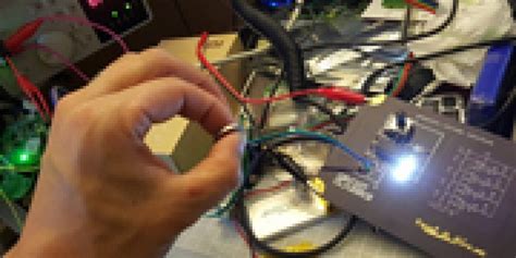
4. In-Circuit Testing (ICT)
In-Circuit Testing (ICT) is a comprehensive testing method that verifies the functionality of individual components and their interconnections on the assembled PCB. ICT uses a bed-of-nails fixture that makes contact with specific test points on the board. The test system then applies stimuli and measures the response to check for:
- Component functionality (resistance, capacitance, inductance, etc.)
- Short circuits or open connections
- Correct component values
- Proper voltage levels
ICT is an effective method for detecting component-level faults and ensuring that the assembled PCB meets the required specifications.
5. Flying Probe Testing
Flying Probe Testing is an alternative to ICT that uses movable probes instead of a fixed bed-of-nails fixture. The probes can move freely over the surface of the PCB and make contact with specific test points. Flying Probe Testing offers several advantages over ICT:
- Flexibility in testing different PCB designs without the need for custom fixtures
- Ability to test both sides of the PCB
- Higher test coverage due to the ability to access hard-to-reach areas
Flying Probe Testing is particularly suitable for low-volume production or prototyping, where the cost of developing a custom ICT fixture may not be justified.
6. Functional Testing
Functional Testing is a system-level testing method that verifies the overall functionality of the assembled PCB. This type of testing involves applying input signals and measuring the output response to ensure that the board performs as intended. Functional Testing can be performed using various methods, such as:
- Edge connector testing
- Boundary scan testing (JTAG)
- Functional test fixtures
- Software-based testing
Functional Testing is essential for validating the complete functionality of the assembled PCB and ensuring that it meets the end-user requirements.
7. Burn-In Testing
Burn-In Testing is a method of subjecting the assembled PCB to elevated temperatures and voltages for an extended period to identify any early-life failures. This type of testing accelerates the aging process and helps to identify components or solder joints that may fail prematurely. Burn-In Testing is particularly useful for products that require high reliability, such as:
- Aerospace and defense applications
- Medical devices
- Automotive electronics
By identifying and eliminating early-life failures, Burn-In Testing helps to improve the overall reliability and quality of the assembled PCBs.
8. Environmental Testing
Environmental Testing involves subjecting the assembled PCB to various environmental stresses to evaluate its performance and reliability under different conditions. Some common environmental tests include:
- Temperature cycling
- Humidity testing
- Vibration and shock testing
- Altitude testing
Environmental Testing helps to ensure that the assembled PCB can withstand the expected operating conditions and maintain its functionality over its intended lifetime.
PCBA Testing Methods Comparison
| Testing Method | Defects Detected | Advantages | Disadvantages |
|---|---|---|---|
| Visual Inspection | Obvious assembly defects | Quick, cost-effective | Limited to visible defects |
| Automated Optical Inspection (AOI) | Component placement, solder joint defects | Fast, reliable, high-volume production | Limited to surface defects |
| X-Ray Inspection | Internal solder joint defects, component placement | Non-destructive, internal structure visibility | Higher cost, limited to specific defect types |
| In-Circuit Testing (ICT) | Component functionality, short/open connections | Comprehensive, component-level testing | Requires custom fixtures, limited test access |
| Flying Probe Testing | Component functionality, short/open connections | Flexible, no custom fixtures, double-sided testing | Slower than ICT, limited test coverage |
| Functional Testing | Overall system functionality | Validates end-user requirements | Requires custom test setup, limited fault isolation |
| Burn-In Testing | Early-life failures, component reliability | Improves reliability, identifies premature failures | Time-consuming, higher cost |
| Environmental Testing | Performance under various environmental conditions | Ensures reliability in expected operating conditions | Requires specialized equipment, time-consuming |
Frequently Asked Questions (FAQ)
1. What is the difference between PCB and PCBA?
PCB (Printed Circuit Board) refers to the bare board without components, while PCBA (Printed Circuit Board Assembly) refers to the board with components soldered onto it.
2. Why is PCBA testing important?
PCBA testing is crucial for ensuring the quality, reliability, and functionality of the assembled PCBs. It helps to identify defects and issues that may affect the performance of the final product.
3. What are the most common defects found during PCBA testing?
Some of the most common defects found during PCBA testing include component placement errors, solder joint defects (bridging, insufficient solder, etc.), missing or damaged components, and incorrect component values.
4. How do I choose the right PCBA testing methods for my product?
The choice of PCBA testing methods depends on various factors, such as the complexity of the PCB, the production volume, the required reliability level, and the available budget. It is recommended to consult with experienced PCBA testing providers to determine the most suitable testing methods for your specific product.
5. Can PCBA testing guarantee a defect-free product?
While PCBA testing can significantly reduce the occurrence of defects and improve the overall quality of the product, it cannot guarantee a 100% defect-free product. Some defects may not be detectable through the available testing methods, and other factors, such as component quality and handling, can also impact the final product quality.
Conclusion
PCBA testing is an essential part of the electronics manufacturing process, ensuring that the assembled PCBs meet the required quality, reliability, and performance standards. The eight testing methods discussed in this article – Visual Inspection, Automated Optical Inspection (AOI), X-Ray Inspection, In-Circuit Testing (ICT), Flying Probe Testing, Functional Testing, Burn-In Testing, and Environmental Testing – each offer unique advantages and capabilities in detecting various types of defects and validating the functionality of the assembled PCBs.
By implementing a comprehensive PCBA testing strategy that incorporates the appropriate combination of these methods, manufacturers can significantly reduce the occurrence of defects, improve the overall quality and reliability of their products, and minimize the risk of costly failures in the field. As the complexity of electronic devices continues to increase, the importance of thorough and effective PCBA testing will only continue to grow, making it a critical consideration for any electronics manufacturing operation.
No responses yet