Introduction
Printed Circuit Boards (PCBs) are the backbone of modern electronics, enabling the interconnection of various components to create complex circuits. However, even with advancements in manufacturing processes, PCBs are not immune to issues that can affect their performance and reliability. In this article, we will discuss four common issues in PCBs or PCB pads and provide solutions for PCB Troubleshooting.
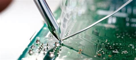
1. Solder Bridging
What is Solder Bridging?
Solder bridging, also known as solder shorts, occurs when excess solder creates an unintended connection between two or more pads or traces on a PCB. This can lead to short circuits, causing the circuit to malfunction or even damage the components.
Causes of Solder Bridging
- Excessive solder: Applying too much solder during the soldering process can cause it to flow and create bridges between adjacent pads or traces.
- Improper solder mask design: If the solder mask opening is too large or misaligned, it can allow solder to flow beyond the intended area.
- Insufficient spacing: If the pads or traces are placed too close together, the risk of solder bridging increases.
How to Fix Solder Bridging
- Use a soldering iron with a fine tip to carefully remove the excess solder.
- Apply flux to the affected area to help the solder flow away from the bridge.
- If the bridge persists, use solder wick or a desoldering pump to remove the excess solder.
- Inspect the PCB design and consider increasing the spacing between pads or traces to prevent future bridging issues.
| Solder Bridging | Cause | Solution |
|---|---|---|
| Excess solder | Applying too much solder | Remove excess solder with a fine-tipped iron |
| Improper mask | Oversized solder mask opening | Adjust solder mask design to reduce opening size |
| Insufficient spacing | Pads/traces too close | Increase spacing between pads/traces in PCB design |

2. Lifted Pads
What are Lifted Pads?
Lifted pads occur when the copper pad on a PCB separates from the board’s surface. This can happen during the soldering process or due to mechanical stress on the board. Lifted pads can cause intermittent connections or complete loss of connectivity, leading to circuit failures.
Causes of Lifted Pads
- Excessive heat during soldering: Applying too much heat or prolonged exposure to heat can cause the pad to lift from the board.
- Mechanical stress: Rough handling, vibration, or bending of the PCB can cause pads to lift.
- Poor adhesion: If the copper pad is not properly bonded to the PCB substrate, it may be more susceptible to lifting.
How to Fix Lifted Pads
- If the pad is only partially lifted, carefully apply a small amount of epoxy or superglue under the pad to reattach it to the board.
- For completely lifted pads, remove the component and clean the area around the pad.
- Create a new pad by applying a small amount of solder to the exposed trace and flattening it with a soldering iron.
- Solder the component back onto the new pad, ensuring a secure connection.
| Lifted Pads | Cause | Solution |
|---|---|---|
| Partial lift | Excessive heat or stress | Apply epoxy or superglue to reattach the pad |
| Complete lift | Poor adhesion or handling | Create a new pad with solder and reattach component |

3. Dry Joints
What are Dry Joints?
Dry joints, also known as Cold Solder Joints, occur when the solder fails to properly bond with the pad or component lead. This can result in a weak or intermittent connection, leading to circuit failures or unreliable performance.
Causes of Dry Joints
- Insufficient heat: If the soldering iron temperature is too low or not applied long enough, the solder may not flow properly, resulting in a dry joint.
- Contamination: Dirt, grease, or oxidation on the pad or component lead can prevent the solder from bonding properly.
- Improper solder composition: Using solder with the wrong alloy composition can lead to poor bonding and dry joints.
How to Fix Dry Joints
- Remove the component and clean the pad and component lead with isopropyl alcohol to remove any contaminants.
- Apply a small amount of fresh solder to the pad and component lead.
- Use a soldering iron with the appropriate temperature and apply heat to the joint until the solder flows smoothly.
- Allow the joint to cool and solidify before inspecting it for proper bonding.
| Dry Joints | Cause | Solution |
|---|---|---|
| Insufficient heat | Low iron temperature | Adjust iron temperature and apply heat adequately |
| Contamination | Dirt, grease, or oxidation | Clean pad and lead with isopropyl alcohol |
| Improper solder | Wrong alloy composition | Use solder with the correct composition |

4. Tombstoning
What is Tombstoning?
Tombstoning, also known as drawbridging, is a phenomenon that occurs during the reflow soldering process, particularly with surface-mount devices (SMDs). It happens when one end of a component lifts off the pad, standing upright like a tombstone. This results in an open circuit and can cause the component to fail.
Causes of Tombstoning
- Uneven heating: If one pad heats up faster than the other, the surface tension of the molten solder can pull the component upright.
- Misaligned component placement: If the component is not placed correctly on the pads, it may be more susceptible to tombstoning.
- Insufficient solder paste: If there is not enough solder paste on the pads, the component may not be held securely in place during reflow.
How to Fix Tombstoning
- Ensure even heating during the reflow process by using a properly calibrated reflow oven or adjusting the temperature profile.
- Verify that the component placement is accurate and the pads are properly aligned.
- Apply an adequate amount of solder paste to the pads to ensure a strong bond between the component and the board.
- If tombstoning has already occurred, remove the affected component and clean the pads before replacing it with a new component.
| Tombstoning | Cause | Solution |
|---|---|---|
| Uneven heating | One pad heats faster | Ensure even heating during reflow |
| Misalignment | Improper component placement | Verify accurate component placement and alignment |
| Insufficient solder | Not enough solder paste | Apply adequate solder paste to the pads |
Frequently Asked Questions (FAQ)
1. Can I fix solder bridging without removing the component?
In some cases, yes. If the solder bridge is small and accessible, you can carefully use a soldering iron with a fine tip to remove the excess solder. However, if the bridge is large or difficult to access, it may be necessary to remove the component to properly clean and resolder the pads.
2. Is it possible to prevent lifted pads?
While it may not be possible to completely eliminate the risk of lifted pads, you can take steps to minimize their occurrence. These include:
- Using the appropriate soldering temperature and duration
- Handling PCBs with care to avoid mechanical stress
- Ensuring proper adhesion between the copper pads and the PCB substrate during manufacturing
3. Can dry joints cause intermittent circuit failures?
Yes, dry joints can cause intermittent circuit failures. Due to the weak or improper bonding between the solder and the pad or component lead, the connection may be unstable. This can lead to intermittent connectivity issues, which can be difficult to diagnose and repair.
4. How can I identify tombstoning on my PCB?
Tombstoning is usually visible to the naked eye. You will see a component standing upright on one end, with the other end lifted off the pad. In some cases, you may need to use a magnifying glass or microscope to confirm the presence of tombstoning, particularly with smaller SMD components.
5. Can I reuse a component that has been affected by tombstoning?
It is generally not recommended to reuse a component that has been affected by tombstoning. The upright position of the component may have caused stress or damage to its leads or internal structure. It is best to remove the affected component and replace it with a new one to ensure reliable performance.
Conclusion
PCB troubleshooting is an essential skill for anyone working with electronic circuits. By understanding common issues such as solder bridging, lifted pads, dry joints, and tombstoning, you can quickly identify and resolve problems that may affect the performance and reliability of your PCBs. Remember to practice proper soldering techniques, use the appropriate tools and materials, and follow best practices in PCB design to minimize the occurrence of these issues. With patience and attention to detail, you can effectively troubleshoot and repair PCBs, ensuring the smooth operation of your electronic devices.
No responses yet