Introduction to 3D-printed PCBs
3D printing has revolutionized the way we manufacture products, and now it’s making its way into the world of electronics. With the advent of 3D-printed PCBs (Printed Circuit Boards), designers and engineers can create custom, high-quality circuit boards faster and more cost-effectively than ever before. This article will explore the process of 3D printing PCBs, the advantages it offers, and how to generate printing models for your designs.
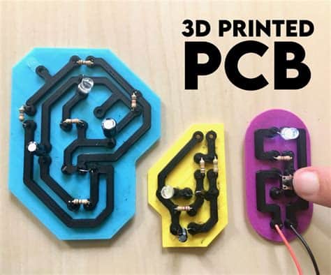
What are 3D-Printed PCBs?
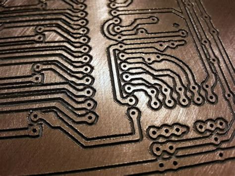
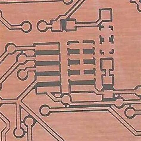
3D-printed PCBs are circuit boards created using additive manufacturing techniques, such as Fused Deposition Modeling (FDM) or Stereolithography (SLA). Unlike traditional PCB manufacturing methods, which involve subtractive processes like etching and drilling, 3D printing builds the circuit board layer by layer, depositing conductive and insulating materials as needed.
Advantages of 3D-Printed PCBs
- Rapid Prototyping: 3D printing allows for quick and easy prototyping of PCB designs, reducing the time and cost associated with traditional manufacturing methods.
- Customization: With 3D printing, designers can create complex, custom-shaped PCBs that would be difficult or impossible to manufacture using conventional techniques.
- Reduced Waste: 3D printing is an additive process, meaning it only uses the material needed for the final product, minimizing waste and environmental impact.
- Integration with Other Components: 3D-printed PCBs can be designed to integrate seamlessly with other 3D-printed components, such as enclosures and mechanical parts.
The Process of 3D Printing PCBs
Designing the PCB
The first step in 3D printing a PCB is to design the circuit board using CAD (Computer-Aided Design) software. Popular PCB design software includes:
- Autodesk Eagle
- KiCad
- Altium Designer
When designing the PCB, consider the following factors:
- Component placement and routing
- Layer stackup and thickness
- Conductive and insulating material properties
- Printing resolution and accuracy
Preparing the 3D Printing Files
Once the PCB design is complete, it needs to be exported in a format suitable for 3D printing. The most common file formats for 3D printing are:
- STL (Standard Tessellation Language)
- OBJ (Object File Format)
- AMF (Additive Manufacturing File Format)
Most PCB design software can export the design in one or more of these formats. It’s essential to ensure that the exported file accurately represents the PCB design and is compatible with the chosen 3D printing technology.
Choosing the 3D Printing Technology
There are several 3D printing technologies available for creating PCBs, each with its own advantages and limitations. The most common technologies are:
- Fused Deposition Modeling (FDM): FDM printers use a heated nozzle to extrude thermoplastic filament, building the PCB layer by layer. FDM is relatively inexpensive and widely available but may have limitations in terms of resolution and material properties.
- Stereolithography (SLA): SLA printers use a laser to cure and harden liquid resin, creating highly detailed and accurate prints. SLA is more expensive than FDM but offers superior resolution and surface finish.
- Selective Laser Sintering (SLS): SLS printers use a laser to sinter powdered materials, such as nylon or metal, into a solid object. SLS is capable of producing strong, durable parts but is more expensive and less widely available than FDM or SLA.
| Technology | Advantages | Disadvantages |
|---|---|---|
| FDM | – Inexpensive – Widely available |
– Limited resolution – Material property limitations |
| SLA | – High resolution – Excellent surface finish |
– More expensive than FDM – Limited material options |
| SLS | – Strong, durable parts – Variety of materials |
– Expensive – Less widely available |
Printing the PCB
Once the 3D printing files are prepared and the technology is chosen, the PCB can be printed. The printing process will vary depending on the selected technology but generally involves the following steps:
- Loading the 3D printing files into the printer software
- Preparing the printer by loading the appropriate materials and calibrating the settings
- Initiating the print and monitoring the progress
- Post-processing the printed PCB, which may include cleaning, curing, or assembling multiple parts
Generating Printing Models
To successfully 3D print a PCB, it’s crucial to generate accurate and optimized printing models. Here are some tips for creating high-quality printing models:
Optimize the PCB Design for 3D Printing
When designing the PCB, keep in mind the limitations and capabilities of the chosen 3D printing technology. Consider factors such as minimum feature size, layer thickness, and material properties. Optimize the design to minimize overhangs, support structures, and other potential printing issues.
Use Appropriate Software Tools
Several software tools are available to help generate printing models for 3D-printed PCBs. Some popular options include:
- Autodesk Netfabb
- Slic3r
- Cura
These tools can help optimize the PCB design for 3D printing, generate support structures, and slice the model into layers for printing.
Validate the Printing Model
Before sending the printing model to the printer, it’s essential to validate it for accuracy and printability. Use the printer software’s built-in validation tools or standalone software like Meshmixer to check for potential issues, such as:
- Thin walls or unsupported structures
- Overlapping or intersecting geometry
- Non-manifold edges or vertices
Addressing these issues before printing can save time and materials and ensure a successful print.

FAQ
-
Q: Can 3D-printed PCBs be used for high-frequency applications?
A: While 3D-printed PCBs can be used for high-frequency applications, their performance may be limited compared to conventionally manufactured PCBs. The conductive and insulating materials used in 3D printing may have different dielectric properties, which can affect signal integrity and electromagnetic compatibility. -
Q: Are 3D-printed PCBs suitable for mass production?
A: Currently, 3D-printed PCBs are more suitable for prototyping and low-volume production runs. Mass production using 3D printing may not be as cost-effective or efficient as traditional PCB manufacturing methods, such as etching or milling. -
Q: What materials can be used for 3D printing PCBs?
A: Various materials can be used for 3D printing PCBs, depending on the chosen technology. FDM printers typically use thermoplastics like PLA or ABS, which can be mixed with conductive fillers like graphene or metal particles. SLA and SLS printers can use photopolymers or powdered materials, respectively, which can also be infused with conductive additives. -
Q: How durable are 3D-printed PCBs compared to conventionally manufactured ones?
A: The durability of 3D-printed PCBs depends on the materials and technology used. Generally, 3D-printed PCBs may not be as durable as conventionally manufactured PCBs, particularly in terms of mechanical strength and thermal stability. However, advances in materials and printing techniques are continually improving the durability of 3D-printed PCBs. -
Q: Can 3D-printed PCBs be used for flexible circuits?
A: Yes, 3D printing can be used to create flexible PCBs. Some 3D printing technologies, such as FDM and SLA, can use flexible materials like thermoplastic polyurethane (TPU) or elastic resins to produce flexible circuits. However, the performance and reliability of 3D-printed flexible PCBs may not be as high as conventionally manufactured flexible PCBs.
Conclusion
3D printing PCBs offers a new and exciting approach to electronic circuit design and manufacturing. With the ability to create custom, complex-shaped PCBs rapidly and cost-effectively, 3D printing is poised to transform the way we develop and produce electronic devices. By understanding the process of 3D printing PCBs, choosing the appropriate technology, and generating optimized printing models, designers and engineers can harness the power of this innovative manufacturing technique to bring their ideas to life.
As 3D printing technologies continue to evolve and improve, we can expect to see even more applications for 3D-printed PCBs in various industries, from consumer electronics to aerospace and beyond. By staying up-to-date with the latest developments in this field and experimenting with new materials and techniques, designers and engineers can push the boundaries of what’s possible with 3D-printed PCBs and create the next generation of electronic devices.
No responses yet