Introduction to 3D-printed PCBs
3D printing technology has revolutionized the way we create physical objects, allowing for rapid prototyping and customization. In recent years, this technology has been applied to the field of electronics, enabling the creation of 3D-printed PCBs (Printed Circuit Boards). These innovative circuit boards offer several advantages over traditional PCB manufacturing methods, making them an attractive option for fast prototyping and small-scale production.
What are 3D-Printed PCBs?
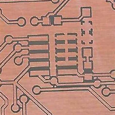
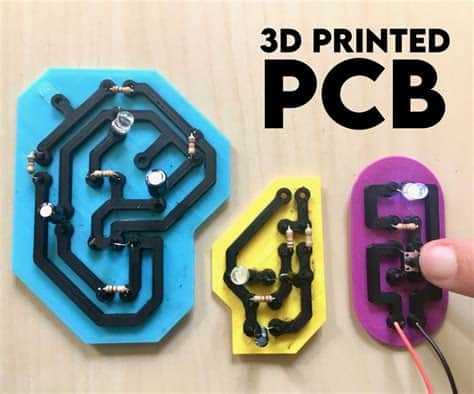
3D-printed PCBs are circuit boards that are created using additive manufacturing techniques, specifically 3D printing. Instead of etching copper traces on a substrate, conductive materials are deposited layer by layer to form the desired circuit pattern. This process allows for greater flexibility in design and faster turnaround times compared to conventional PCB fabrication methods.
Advantages of 3D-Printed PCBs
-
Rapid Prototyping: 3D-printed PCBs can be created much faster than traditional PCBs, enabling quick iterations and design refinements.
-
Customization: With 3D printing, circuit boards can be tailored to specific applications, allowing for unique shapes, sizes, and features.
-
Cost-Effective: For small quantities and prototypes, 3D-printed PCBs can be more economical than traditional PCB manufacturing methods.
-
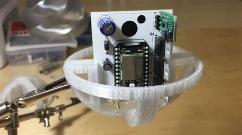
Integrated Functionality: 3D printing allows for the integration of mechanical and electrical components, creating more compact and functional devices.
Types of 3D Printing Technologies for PCBs
Several 3D printing technologies can be used to create PCBs, each with its own advantages and limitations.
Fused Deposition Modeling (FDM)
FDM is the most common and affordable 3D printing technology. It involves extruding a molten thermoplastic material through a nozzle to build up the object layer by layer. For PCBs, a conductive filament, such as a composite of PLA and graphene, is used to create the conductive traces.
| Advantages | Disadvantages |
|---|---|
| Low cost | Lower resolution compared to other methods |
| Widely available | Limited material options |
| Easy to use | Requires post-processing |
Stereolithography (SLA)
SLA uses a UV laser to cure and harden liquid resin layer by layer. For PCBs, a conductive resin is used to create the traces. After printing, the board is cleaned and cured in a UV oven.
| Advantages | Disadvantages |
|---|---|
| High resolution | More expensive than FDM |
| Smooth surface finish | Limited material options |
| Good for fine details | Requires post-processing |
Selective Laser Sintering (SLS)
SLS uses a high-power laser to sinter powdered materials, binding them together to create a solid object. For PCBs, a conductive powder, such as a mixture of nylon and copper, is used to create the traces.
| Advantages | Disadvantages |
|---|---|
| High strength and durability | Expensive equipment |
| Good for complex geometries | Rough surface finish |
| Wide range of materials | Requires post-processing |
Design Considerations for 3D-Printed PCBs
When designing 3D-printed PCBs, several factors must be taken into account to ensure optimal performance and manufacturability.
Material Selection
Choosing the right conductive material is crucial for the performance of 3D-printed PCBs. Common materials include:
- Conductive PLA (Polylactic Acid) filament
- Conductive ABS (Acrylonitrile Butadiene Styrene) filament
- Conductive resin
- Conductive powder (e.g., a mixture of nylon and copper)
The selection of the material depends on the 3D printing technology being used, the desired electrical properties, and the mechanical requirements of the PCB.
Trace Width and Spacing
When designing 3D-printed PCBs, it is important to consider the minimum trace width and spacing that can be achieved with the chosen 3D printing technology. FDM typically has a lower resolution compared to SLA and SLS, which means that thicker traces and larger spacings may be required.
| 3D Printing Technology | Typical Minimum Trace Width | Typical Minimum Spacing |
|---|---|---|
| FDM | 0.5 mm | 0.5 mm |
| SLA | 0.1 mm | 0.1 mm |
| SLS | 0.2 mm | 0.2 mm |
Layer Thickness
The layer thickness of a 3D-printed PCB affects its electrical properties and surface finish. Thinner layers generally result in smoother surfaces and better electrical performance, but they also increase the printing time. A balance must be struck between print quality and speed.
| 3D Printing Technology | Typical Layer Thickness Range |
|---|---|
| FDM | 50 – 400 microns |
| SLA | 25 – 100 microns |
| SLS | 50 – 150 microns |
Post-Processing
After printing, 3D-printed PCBs often require post-processing to improve their electrical and mechanical properties. This may include:
- Cleaning: Removing support materials and residues from the printing process.
- Curing: Exposing the PCB to UV light or heat to fully cure the conductive material.
- Polishing: Smoothing the surface of the PCB to improve electrical contact and reduce signal loss.
- Coating: Applying a protective coating to the PCB to improve durability and insulation.

Applications of 3D-Printed PCBs
3D-printed PCBs have found applications in various fields, ranging from hobbyist projects to industrial prototypes.
Rapid Prototyping
One of the main advantages of 3D-printed PCBs is their ability to quickly create functional prototypes. This allows designers and engineers to test and refine their designs in a short amount of time, reducing development costs and time-to-market.
Customized Electronics
3D printing enables the creation of customized electronic devices tailored to specific applications. This is particularly useful in fields such as wearable technology, where the form factor and functionality of the device must be adapted to the user’s needs.
Education and Research
3D-printed PCBs are also valuable tools for education and research. They allow students and researchers to quickly and easily create custom circuits for experiments and projects, fostering innovation and hands-on learning.
Future Developments in 3D-Printed PCBs
As 3D printing technology continues to advance, we can expect to see further developments in the field of 3D-printed PCBs.
Improved Materials
Researchers are constantly developing new conductive materials with better electrical and mechanical properties. These materials will enable the creation of more complex and high-performance 3D-printed PCBs.
Multi-Material Printing
The ability to print multiple materials simultaneously will allow for the integration of additional functionality into 3D-printed PCBs, such as embedded sensors, antennas, and heat sinks.
Increased Automation
As the demand for 3D-printed PCBs grows, we can expect to see more automated solutions for their design and production. This will include software tools for optimizing PCB layouts and automated post-processing equipment.
Frequently Asked Questions (FAQ)
-
Q: How durable are 3D-printed PCBs compared to traditional PCBs?
A: The durability of 3D-printed PCBs depends on the materials and printing technology used. In general, they may not be as durable as traditional PCBs, but they are sufficient for prototyping and low-stress applications. Proper post-processing and protective coatings can improve their durability. -
Q: Can 3D-printed PCBs be used for high-frequency applications?
A: 3D-printed PCBs can be used for high-frequency applications, but their performance may be limited by the resolution and electrical properties of the conductive materials used. SLA and SLS technologies typically offer better high-frequency performance compared to FDM. -
Q: Are 3D-printed PCBs suitable for mass production?
A: Currently, 3D-printed PCBs are not well-suited for mass production due to their longer printing times and higher costs compared to traditional PCB manufacturing methods. However, they are ideal for small-scale production and rapid prototyping. -
Q: Can 3D-printed PCBs be soldered using standard soldering techniques?
A: Yes, 3D-printed PCBs can be soldered using standard soldering techniques, such as reflow soldering and hand soldering. However, the heat resistance of the PCB material should be considered to avoid deformation or damage during the soldering process. -
Q: Are there any environmental concerns associated with 3D-printed PCBs?
A: The environmental impact of 3D-printed PCBs depends on the materials used and the disposal methods employed. Some conductive materials may contain hazardous substances, and proper disposal procedures should be followed. However, 3D printing can reduce waste compared to traditional PCB manufacturing methods, as it allows for on-demand production and minimizes the need for large inventories.
Conclusion
3D-printed PCBs offer a promising solution for rapid prototyping and customized electronics. By leveraging the advantages of additive manufacturing, designers and engineers can create functional circuit boards quickly and cost-effectively. As 3D printing technology continues to evolve, we can expect to see further improvements in the performance and applicability of 3D-printed PCBs.
While they may not replace traditional PCB manufacturing methods for mass production, 3D-printed PCBs have already proven their value in various fields, from hobbyist projects to industrial prototypes. As research into new materials and processes continues, the potential of 3D-printed PCBs will only grow, opening up new possibilities for innovation and customization in the world of electronics.
No responses yet