
Introduction to PCB Essentials
Printed Circuit Boards (PCBs) are the backbone of modern electronics. They provide a platform for electrical components to be mounted and connected, enabling the creation of complex circuits that power our devices. In this comprehensive article, we will dive deep into the world of 2 layer PCBs, covering everything you need to know to understand and work with these essential components.
What is a 2 Layer PCB?
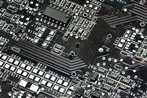
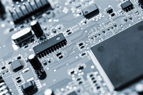
A 2 layer PCB is a printed circuit board that consists of two conductive layers, typically made of copper, separated by an insulating substrate. The two layers are used for routing electrical signals and power between components. The top layer is usually reserved for components and signal traces, while the bottom layer is used for ground and power planes.
Advantages of 2 Layer PCBs
2 layer PCBs offer several advantages over single layer boards:
- Increased circuit density: With two layers, more components can be packed into a smaller space, allowing for more complex circuits in a compact form factor.
- Improved signal integrity: The ground plane on the bottom layer helps to reduce electromagnetic interference (EMI) and improve signal quality.
- Better power distribution: The power plane on the bottom layer provides a low-impedance path for distributing power to components, reducing voltage drop and improving overall circuit performance.
- Lower cost: 2 layer PCBs are generally less expensive than multi-layer boards, making them a cost-effective choice for many applications.
Designing 2 Layer PCBs
PCB Design Software
To design a 2 layer PCB, you will need to use specialized PCB design software. Some popular options include:
- Altium Designer
- KiCad
- Eagle
- OrCAD
- Mentor Graphics PADS
These software packages provide a range of tools for schematic capture, component placement, and routing, as well as features for design rule checking (DRC) and generating manufacturing files.
PCB Design Guidelines
When designing a 2 layer PCB, there are several key guidelines to follow to ensure optimal performance and manufacturability:
- Component placement: Place components in a logical and organized manner, keeping related components close together and minimizing the distance between connected pins.
- Trace width and spacing: Choose appropriate trace widths based on the current carrying requirements of the circuit, and ensure that traces are spaced sufficiently apart to avoid short circuits and signal interference.
- Via placement: Use vias strategically to connect traces between layers, minimizing the number of vias where possible to reduce manufacturing costs and improve reliability.
- Ground and power planes: Create solid ground and power planes on the bottom layer to provide a low-impedance path for current and reduce EMI.
- Design rule checking: Use the DRC tools provided by your PCB design software to check for errors and ensure that your design meets manufacturing requirements.
PCB Layer Stackup
The layer stackup of a 2 layer PCB typically consists of the following:
| Layer | Material | Thickness |
|---|---|---|
| Top Copper | Copper | 1 oz (35 μm) |
| Substrate | FR-4 | 1.6 mm |
| Bottom Copper | Copper | 1 oz (35 μm) |
| Solder Mask | Epoxy | 0.0254 mm |
| Silkscreen | Epoxy | 0.0254 mm |
The substrate is usually made of FR-4, a glass-reinforced epoxy laminate material that provides good insulation and mechanical strength. The copper layers are typically 1 oz (35 μm) thick, although thicker copper can be used for high-current applications. The solder mask and silkscreen layers are applied over the copper layers to protect the board and provide labeling and identification.
Manufacturing 2 Layer PCBs
PCB Fabrication Process
The process of manufacturing a 2 layer PCB involves several steps:
- Film generation: The PCB design files are used to generate photographic films for each layer of the board.
- Etching: The films are used to selectively etch away unwanted copper from the substrate, leaving behind the desired circuit pattern.
- Drilling: Holes are drilled through the board to accommodate through-hole components and vias.
- Plating: The holes are plated with copper to provide electrical connectivity between layers.
- Solder mask application: A protective solder mask layer is applied over the copper layers to prevent short circuits and improve solderability.
- Silkscreen printing: Labels and identifiers are printed onto the board using a silkscreen process.
- Surface finish: A surface finish, such as HASL (Hot Air Solder Leveling) or ENIG (Electroless Nickel Immersion Gold), is applied to protect the exposed copper and improve solderability.
PCB Manufacturing Considerations
When manufacturing 2 layer PCBs, there are several key considerations to keep in mind:
- Minimum feature size: The minimum trace width and spacing, as well as the minimum drill hole size, are determined by the capabilities of the PCB manufacturer. It is important to design your board with these limitations in mind.
- Panelization: PCBs are often manufactured in panels to reduce costs and improve efficiency. Consider panelizing your design to take advantage of these benefits.
- Lead time: The time required to manufacture a PCB can vary depending on the complexity of the design and the workload of the manufacturer. Be sure to plan accordingly and allow sufficient lead time for production.
- Quality control: Work with a reputable PCB manufacturer that has strict quality control measures in place to ensure that your boards are manufactured to the highest standards.

Assembling 2 Layer PCBs
PCB Assembly Techniques
Once your 2 layer PCBs have been manufactured, they need to be assembled with components to create a functional circuit. There are two main techniques for PCB assembly:
- Through-hole assembly: Components with wire leads are inserted into holes drilled through the board and soldered in place on the opposite side.
- Surface-mount assembly: Components are mounted directly onto pads on the surface of the board and soldered in place using a reflow oven.
Surface-mount assembly has largely replaced through-hole assembly in modern electronics due to its higher component density and faster assembly times. However, through-hole assembly is still used for certain components, such as connectors and large power components.
PCB Assembly Process
The process of assembling a 2 layer PCB typically involves the following steps:
- Solder paste application: Solder paste is applied to the pads on the board using a stencil or screen printing process.
- Component placement: Components are placed onto the board, either manually or using an automated pick-and-place machine.
- Reflow soldering: The board is heated in a reflow oven, melting the solder paste and forming a permanent electrical and mechanical connection between the components and the board.
- Inspection and testing: The assembled board is inspected for defects and tested to ensure proper functionality.
PCB Assembly Considerations
When assembling 2 layer PCBs, there are several key considerations to keep in mind:
- Component compatibility: Ensure that the components you are using are compatible with the PCB material and the assembly process.
- Solder paste selection: Choose a solder paste that is appropriate for the size and pitch of the components being used, as well as the reflow temperature profile of the board.
- Reflow profile: Develop a reflow temperature profile that is optimized for the specific components and solder paste being used, taking into account factors such as ramp rate, soak time, and peak temperature.
- Cleaning: After assembly, the board may need to be cleaned to remove flux residue and other contaminants that can affect reliability and performance.
Testing and Debugging 2 Layer PCBs
PCB testing Techniques
Once your 2 layer PCB has been assembled, it is important to test it thoroughly to ensure proper functionality and catch any defects or issues early in the development process. Some common PCB testing techniques include:
- Visual inspection: Visually inspect the board for defects such as solder bridges, cold solder joints, and misaligned components.
- Continuity testing: Use a multimeter to test for continuity between various points on the board, ensuring that connections are properly made and there are no short circuits.
- Functional testing: Apply power to the board and test its functionality, verifying that it performs as intended.
- In-circuit testing: Use specialized test equipment to test individual components and circuits on the board, isolating any issues that may be present.
PCB Debugging Techniques
If issues are found during testing, it may be necessary to debug the board to identify and resolve the problem. Some common PCB debugging techniques include:
- Visual inspection: Carefully inspect the board for any visible defects or issues, such as damaged components or solder bridges.
- Signal tracing: Use an oscilloscope or logic analyzer to trace signals through the board, identifying any areas where the signal is being distorted or interrupted.
- Thermal imaging: Use a thermal camera to identify hot spots on the board that may indicate a short circuit or other issue.
- Component substitution: Swap out individual components to isolate the source of the problem.
PCB Rework and Repair
If issues are found during testing or debugging, it may be necessary to rework or repair the board. Some common PCB rework and repair techniques include:
- Soldering: Use a soldering iron to remove and replace individual components or to repair damaged solder joints.
- Desoldering: Use a desoldering tool, such as a desoldering pump or desoldering wick, to remove solder and components from the board.
- Jumper wires: Use jumper wires to bypass damaged traces or to make temporary connections for testing and debugging purposes.
- Conformal coating: Apply a conformal coating to the board to protect it from moisture and other environmental factors that can cause damage or reliability issues.
Advanced Topics in 2 Layer PCBs
High-Speed Design Considerations
When designing 2 layer PCBs for high-speed applications, there are several additional considerations to keep in mind:
- Impedance control: Ensure that the impedance of the traces on the board is properly controlled to minimize signal reflections and distortion.
- Crosstalk: Minimize crosstalk between adjacent traces by using proper spacing and shielding techniques.
- Grounding: Use a solid ground plane to provide a low-impedance return path for high-speed signals and to minimize EMI.
- Decoupling: Use decoupling capacitors to provide a local source of power for high-speed components and to reduce power supply noise.
Flexible PCBs
Flexible PCBs are a specialized type of 2 layer PCB that are designed to be flexible and bendable. They are commonly used in applications where space is limited or where the board needs to conform to a specific shape or contour. Flexible PCBs are manufactured using a flexible substrate material, such as polyimide, and can be designed with various levels of flexibility and durability depending on the specific application requirements.
PCB material selection
The choice of PCB material can have a significant impact on the performance and reliability of the finished board. Some common PCB materials include:
- FR-4: A glass-reinforced epoxy laminate material that is the most commonly used material for 2 layer PCBs.
- High-Tg FR-4: A variant of FR-4 with a higher glass transition temperature, providing better thermal stability and reliability.
- Polyimide: A flexible substrate material that is commonly used for flexible PCBs.
- Aluminum: A metal-core substrate material that is used for high-power applications where heat dissipation is a concern.
The choice of PCB material will depend on factors such as the operating environment, the electrical and thermal requirements of the circuit, and the cost and availability of the material.
FAQ
- What is the difference between a 2 layer PCB and a 4 layer PCB?
-
A 2 layer PCB has two conductive layers (top and bottom) while a 4 layer PCB has four conductive layers (top, inner 1, inner 2, and bottom). 4 layer PCBs offer higher circuit density and better signal integrity, but are more complex and expensive to manufacture.
-
Can 2 layer PCBs be used for high-speed applications?
-
Yes, 2 layer PCBs can be used for high-speed applications, but they require careful design considerations to ensure proper signal integrity and minimize issues such as crosstalk and EMI. Techniques such as impedance control, grounding, and decoupling can be used to optimize high-speed performance.
-
What is the typical turnaround time for manufacturing a 2 layer PCB?
-
The turnaround time for manufacturing a 2 layer PCB can vary depending on the complexity of the design and the workload of the manufacturer, but is typically in the range of 1-2 weeks for small to medium-sized orders. Rush services may be available for faster turnaround times, but may come at an additional cost.
-
Can 2 layer PCBs be used for flexible applications?
-
Yes, 2 layer PCBs can be designed as flexible PCBs by using a flexible substrate material such as polyimide. Flexible PCBs offer the ability to conform to specific shapes and contours, and are commonly used in applications where space is limited or where the board needs to flex or bend during use.
-
What are some common issues to watch out for when designing 2 layer PCBs?
- Some common issues to watch out for when designing 2 layer PCBs include signal integrity issues such as crosstalk and EMI, power distribution issues such as voltage drop and noise, and manufacturing issues such as minimum feature sizes and drill hole tolerances. Careful design and attention to detail can help minimize these issues and ensure a successful finished product.
Conclusion
2 layer PCBs are a versatile and cost-effective solution for a wide range of electronics applications. By understanding the basics of PCB design, manufacturing, assembly, and testing, you can create high-quality boards that meet your specific requirements and perform reliably in the field. Whether you are a hobbyist or a professional engineer, the skills and knowledge needed to work with 2 layer PCBs are essential for success in today’s fast-paced and ever-evolving electronics industry.
No responses yet