Introduction to PCB Debugging
PCB (Printed Circuit Board) debugging is an essential skill for electronics engineers and hobbyists alike. It involves identifying and resolving issues that arise during the design, fabrication, and assembly of PCBs. Effective PCB debugging can save time, money, and resources by catching problems early in the development process and preventing costly rework or redesigns.
In this comprehensive guide, we will explore various tips, tools, and tricks to help you become a proficient PCB debugger. We will cover topics such as visual inspection, multimeter usage, oscilloscope techniques, thermal imaging, and more. By the end of this article, you will have a solid understanding of the best practices and methodologies for troubleshooting PCBs efficiently and effectively.
The Importance of Visual Inspection
Why Visual Inspection Matters
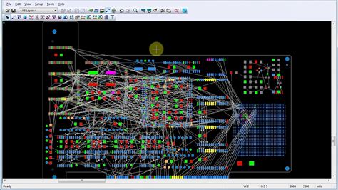
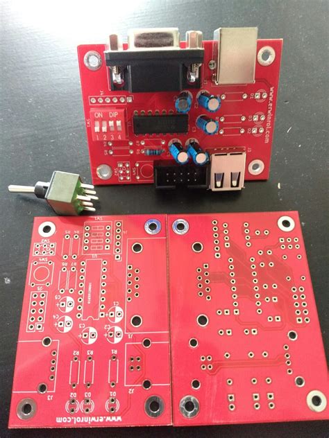
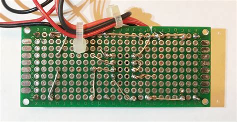
Visual inspection is the first and most crucial step in PCB debugging. It involves carefully examining the PCB for any visible defects, such as:
- Solder bridges
- Cold solder joints
- Damaged components
- Incorrect component placement
- Trace damage or discontinuity
By identifying these issues early on, you can save valuable time and resources that would otherwise be spent on more advanced debugging techniques.
How to Conduct a Thorough Visual Inspection
To perform a comprehensive visual inspection, follow these steps:
- Use a well-lit workspace with a magnifying glass or microscope.
- Check for proper component placement and orientation.
- Inspect solder joints for bridges, cold joints, or insufficient solder.
- Look for any signs of physical damage to components or traces.
- Verify that all necessary components are present and correctly installed.
Common Visual Defects and Their Causes
| Defect | Cause |
|---|---|
| Solder bridges | Excessive solder, improper soldering technique |
| Cold solder joints | Insufficient heat, poor solder wetting |
| Damaged components | Improper handling, electrostatic discharge (ESD) |
| Incorrect component placement | Human error, incorrect bill of materials (BOM) |
| Trace damage or discontinuity | Manufacturing defects, physical stress |
By familiarizing yourself with these common defects and their causes, you can quickly identify and resolve issues during the visual inspection process.
Multimeter Techniques for PCB Debugging
Understanding Multimeter Functionality
A multimeter is an essential tool for PCB debugging, as it allows you to measure various electrical properties, such as:
- Voltage
- Current
- Resistance
- Continuity
By understanding how to use a multimeter effectively, you can pinpoint problems related to power supply, short circuits, open circuits, and component failures.
Measuring Voltage and Current
To measure voltage or current using a multimeter, follow these steps:
- Set the multimeter to the appropriate mode (voltage or current).
- Select the correct range based on the expected value.
- Connect the multimeter probes to the desired test points.
- Read the displayed value and interpret the results.
Checking Continuity and Resistance
Continuity and resistance measurements are useful for identifying short circuits, open circuits, and faulty components. To check continuity or resistance:
- Set the multimeter to the continuity or resistance mode.
- Connect the multimeter probes to the desired test points.
- Observe the displayed value or audible tone (for continuity).
- Compare the results to the expected values for the circuit or component.
Interpreting Multimeter Readings
When interpreting multimeter readings, consider the following:
- Expected voltage, current, or resistance values for the circuit or component
- Tolerance ranges for the measured values
- Possible causes of deviations from the expected values (e.g., faulty components, short circuits, open circuits)
By correctly interpreting multimeter readings, you can quickly identify and isolate problems within the PCB.

Oscilloscope Techniques for PCB Debugging
Understanding Oscilloscope Functionality
An oscilloscope is a powerful tool for visualizing and analyzing time-varying signals in a PCB. It allows you to:
- Observe signal waveforms
- Measure signal characteristics (e.g., frequency, amplitude, rise time)
- Detect signal integrity issues (e.g., noise, distortion, crosstalk)
By mastering oscilloscope techniques, you can effectively debug complex PCB issues related to signal integrity and timing.
Setting Up an Oscilloscope
To set up an oscilloscope for PCB debugging, follow these steps:
- Connect the oscilloscope probes to the desired test points on the PCB.
- Set the appropriate vertical scale (voltage per division) and horizontal scale (time per division) based on the expected signal characteristics.
- Adjust the trigger level and mode to stabilize the displayed waveform.
- Use features such as cursors, measurements, and FFT (Fast Fourier Transform) to analyze the signal in detail.
Analyzing Signal Waveforms
When analyzing signal waveforms on an oscilloscope, consider the following:
- Expected waveform shape and characteristics for the circuit or component
- Presence of noise, distortion, or other signal integrity issues
- Timing relationships between multiple signals (e.g., clock and data)
- Comparison between the observed waveform and the design specifications
By carefully analyzing signal waveforms, you can identify and diagnose issues related to signal integrity, timing, and overall PCB performance.
Common Oscilloscope Measurements
| Measurement | Description |
|---|---|
| Frequency | The number of cycles per second of a periodic signal |
| Amplitude | The maximum and minimum voltage levels of a signal |
| Rise time | The time taken for a signal to transition from a low to a high state |
| Fall time | The time taken for a signal to transition from a high to a low state |
| Pulse width | The duration of a single pulse in a digital signal |
| Duty cycle | The ratio of the pulse width to the total period of a digital signal |
By understanding and utilizing these common oscilloscope measurements, you can effectively characterize and debug PCB signals.
Thermal Imaging for PCB Debugging
Benefits of Thermal Imaging
Thermal imaging is a non-invasive technique that allows you to visualize the temperature distribution across a PCB. This can be particularly useful for identifying:
- Overheating components
- Power dissipation issues
- Thermal design flaws
- Manufacturing defects (e.g., solder voids, insufficient thermal conductivity)
By using thermal imaging, you can quickly locate and address thermal-related problems in your PCB design.
Thermal Imaging Equipment
To perform thermal imaging on a PCB, you will need:
- A thermal camera or infrared thermometer
- Appropriate software for analyzing and interpreting the thermal data
- A controlled environment with minimal external thermal influences
Interpreting Thermal Images
When interpreting thermal images of a PCB, consider the following:
- Expected temperature ranges for components and the overall PCB
- Thermal gradients and hot spots that may indicate design or manufacturing issues
- Correlation between thermal data and other debugging techniques (e.g., multimeter readings, oscilloscope waveforms)
By properly interpreting thermal images, you can identify and resolve thermal-related issues in your PCB design, ensuring optimal performance and reliability.
Advanced PCB Debugging Techniques
In-Circuit Testing (ICT)
In-Circuit Testing (ICT) is an automated testing technique that involves using a bed-of-nails fixture to access and test individual components on a PCB. ICT can help identify:
- Component failures
- Short circuits
- Open circuits
- Incorrect component values
By incorporating ICT into your PCB debugging process, you can quickly isolate and repair component-level issues.
Boundary Scan Testing (BST)
Boundary Scan Testing (BST) is a debugging technique that relies on the IEEE 1149.1 (JTAG) standard. It allows you to test and debug PCBs by accessing and controlling the boundary-scan-enabled components on the board. BST can help:
- Verify connectivity between components
- Identify manufacturing defects
- Program and configure devices
- Perform functional testing
By leveraging BST, you can streamline your PCB debugging process and ensure the proper functioning of boundary-scan-enabled components.
Functional Testing
Functional testing involves verifying that the PCB performs its intended functions under various operating conditions. This can include:
- Power-on self-tests (POST)
- Firmware and software integration tests
- Environmental stress tests (e.g., temperature, humidity, vibration)
By conducting thorough functional testing, you can ensure that your PCB meets its design specifications and performs reliably in its intended environment.
Frequently Asked Questions
What are the most common causes of PCB failures?
The most common causes of PCB failures include:
- Manufacturing defects (e.g., solder bridges, cold solder joints)
- Component failures (e.g., due to overheating, ESD, or aging)
- Design flaws (e.g., signal integrity issues, thermal management problems)
- Environmental factors (e.g., temperature extremes, humidity, vibration)
How can I prevent ESD damage when handling PCBs?
To prevent ESD damage when handling PCBs:
- Use an ESD-safe workspace with grounded mats and wrist straps
- Store PCBs in ESD-safe packaging when not in use
- Avoid touching components or exposed contacts directly
- Use ESD-safe tools and equipment when working on PCBs
What are some best practices for PCB debugging?
Some best practices for PCB debugging include:
- Start with a thorough visual inspection
- Use the appropriate tools for the task at hand (e.g., multimeter, oscilloscope, thermal camera)
- Isolate problems by testing individual components and subsystems
- Document your debugging process and findings for future reference
- Collaborate with other team members and seek advice when needed
How can I improve my PCB debugging skills?
To improve your PCB debugging skills:
- Study PCB design principles and best practices
- Familiarize yourself with common PCB failure modes and their causes
- Practice using debugging tools and techniques on sample PCBs
- Participate in online forums and communities to learn from experienced professionals
- Attend workshops, seminars, or courses on PCB debugging and troubleshooting
What should I do if I cannot identify the root cause of a PCB problem?
If you cannot identify the root cause of a PCB problem:
- Revisit your debugging process and double-check your findings
- Consult with colleagues or experts in the field for a fresh perspective
- Consider alternative debugging techniques or tools that you may have overlooked
- Reevaluate your assumptions about the PCB design and functionality
- As a last resort, consider redesigning the problematic portion of the PCB
Conclusion
PCB debugging is a critical skill for anyone involved in electronics design and manufacturing. By understanding and applying the tips, tools, and tricks covered in this article, you can become a more effective and efficient PCB debugger. Remember to start with a visual inspection, use the appropriate tools for the task at hand, and follow best practices to ensure a systematic and thorough debugging process.
As you continue to develop your PCB debugging skills, stay curious, and never stop learning. Keep up with the latest industry trends, participate in community discussions, and share your knowledge with others. With practice and perseverance, you will be well on your way to mastering the art of PCB debugging.
No responses yet