1. Understand and Specify Controlled Impedances
The first step in avoiding signal integrity issues is to clearly understand and specify the target impedances for your PCB traces and interconnects. Some common controlled impedances used are:
| Impedance | Typical Use Case |
|---|---|
| 50 ohms | RF circuits, high-speed digital |
| 75 ohms | Video, telecommunications |
| 90-120 ohms | Differential signals (USB, LVDS, etc.) |
Work with your PCB fabricator early in the design process to communicate your impedance requirements and understand their capabilities and limitations in terms of materials, trace geometries, and layer stackup to achieve your targets.
2. Use Appropriate Dielectric Materials
The choice of PCB dielectric material significantly impacts the characteristic impedance of traces. Some key material properties to consider are:
- Dielectric constant (Dk): Affects the capacitance and velocity of propagation. Lower Dk enables thinner dielectrics and traces for a given impedance.
- Loss tangent (Df): Determines the amount of absorption loss. Lower loss tangents are crucial at higher frequencies.
- Consistency and stability: Variations in dielectric properties can cause impedance mismatches. Using consistent, stable materials is important.
Some commonly used dielectric materials and their properties:
| Material | Dk | Df | Frequency |
|---|---|---|---|
| FR-4 | 4.2-4.5 | 0.018-0.025 | < 5 GHz |
| Rogers 4350B | 3.48 | 0.0031 | 8-10 GHz |
| Isola I-Tera MT40 | 3.45-3.75 | 0.0011-0.0018 | < 40 GHz |
3. Optimize Trace Geometry
The width, thickness, and spacing of PCB traces directly affect their characteristic impedance. Thinner traces have higher impedance, while thicker traces have lower impedance. Some guidelines for trace geometry:
- Use trace width calculators or lookup tables to determine the right width for your desired impedance and board stackup.
- Maintain consistent trace widths and spacing as much as possible. Avoid abrupt changes that can cause discontinuities.
- If needed, gradually taper or “neck down” traces when changing widths to minimize impedance mismatches.
- Maintain symmetry in differential traces to ensure equal impedances and avoid Mode Conversion.

4. Control Return Paths
Providing a clear, uninterrupted reference plane for return currents is essential for maintaining trace impedance and minimizing crosstalk or EMI. Some tips:
- Use ground planes next to signal layers to provide a low-impedance return path.
- Maintain the plane area under traces. Avoid cuts or splits in planes that can disrupt return paths.
- Use stitching vias to connect segmented planes at regular intervals to equalize potentials.
- Place ground vias near connectors or components to provide a short return path.
5. Match Component and Trace Impedances
Impedance mismatches between PCB traces and components like connectors, packages, or loads can cause reflections. To minimize discontinuities:
- Choose components with impedances matching your system (e.g., 50-ohm connectors/terminations for 50-ohm traces).
- Use component datasheets or models to understand their parasitics and impedances at your frequencies of interest.
- Perform simulations or calculations to determine the impact of mismatches and adjust component selection or placement if needed.
- Consider impedance-matching networks or terminations to improve matching between components and traces.
6. Terminate Transmission Lines Properly
Proper termination of PCB traces is crucial to preventing reflections from unterminated ends. The two main termination types are:
- Series termination: A resistor equal to the trace impedance is placed near the driver. This absorbs reflections from the far end.
- Parallel termination: A resistor equal to the trace impedance is placed at the far end (receiver) to prevent reflections back to the source.
The choice of termination depends on factors like trace length, signal rise/fall times, and driver impedance. Some tips:
- Use series termination for short traces or to minimize power consumption when drivers are mismatched.
- Use parallel termination for traces longer than half the signal rise time to minimize far-end reflections.
- Consider adjustable or active terminations for variable impedances or to save power.
7. Manage Discontinuities
While it’s best to avoid impedance discontinuities altogether, sometimes they are unavoidable due to space constraints, layer transitions, or other factors. Some ways to manage discontinuities:
- Minimize the use of vias, especially for high-frequency signals. If needed, use microvias to minimize Parasitic Inductance.
- Avoid unnecessary routing of traces through connectors, packages, or breakouts that can add discontinuities.
- Use stitching capacitors near plane splits or breaks to provide AC continuity for return paths.
- Perform simulations to understand the impact of discontinuities and adjust the design as needed.
8. Simulate and Measure Impedances
To ensure your controlled impedance design is effective, it’s important to simulate and measure impedances at various stages:
- Use field solvers or calculator tools to estimate impedances based on your stackup and trace geometries.
- Perform pre-layout simulations to validate impedance targets and identify potential issues.
- After layout, use a 2D or 3D solver to extract parasitic impedances and analyze discontinuities.
- Measure test coupons or sample boards to verify actual fabricated impedances meet your specifications.
- Consider time-domain reflectometry (TDR) measurements to characterize impedance profiles along traces.
9. Decouple Power and Ground
Proper Power Integrity is also important for maintaining consistent trace and component impedances. Poor decoupling can allow power/ground noise to modulate impedances. Some guidelines:
- Use adequate decoupling capacitors near ICs and other components to reduce power supply impedance at high frequencies.
- Place decoupling capacitors close to power pins to minimize loop inductance.
- Use multiple capacitor values (e.g., bulk, ceramic, and package) to provide broadband decoupling.
- Simulate power distribution networks to analyze impedances and optimize decoupling placement.
10. Document and Communicate Requirements
Lastly, it’s crucial to clearly document and communicate your impedance requirements to all stakeholders, including PCB designers, manufacturers, and assembly houses. Some tips:
- Specify controlled impedances, materials, and stackups in design files and fab drawings.
- Provide detailed trace width/spacing tables and calculations to your manufacturer.
- Define acceptable impedance tolerances (e.g., ±10%) and how they will be measured.
- Review impedance coupon designs and measurements with your manufacturer to ensure compliance.
- Archive all design files, specifications, and measurements for future reference and troubleshooting.
Frequently Asked Questions
1. What is impedance control and why is it important?
Impedance control is the practice of designing PCB traces and interconnects to have specific, consistent characteristic impedances. It is important for maintaining good signal integrity, minimizing reflections, and ensuring proper termination of high-speed signals. Without proper impedance control, signals can suffer from distortions, ringing, crosstalk, and other issues that can cause data errors or system malfunctions.
2. What factors affect the characteristic impedance of a PCB trace?
The main factors that determine the characteristic impedance of a PCB trace are:
- The dielectric constant of the PCB material
- The thickness and width of the trace
- The distance between the trace and the reference (ground or power) plane
- The presence of other traces or components nearby
By carefully choosing materials and geometries, designers can achieve specific target impedances.
3. What are some common PCB materials used for impedance control?
Some common PCB materials and their typical applications are:
- FR-4: Low-cost, general-purpose material for digital circuits up to a few GHz
- Rogers RO4000 series: Low-loss, high-frequency materials for RF and microwave applications
- Isola I-Tera: Very low-loss material for high-speed digital and RF applications up to 40 GHz
- PTFE (Teflon): Extremely low-loss material for demanding RF and microwave applications
The choice of material depends on the frequency, loss, and cost requirements of the design.
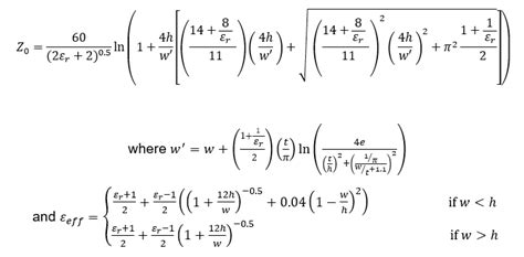
4. How can I calculate the impedance of a PCB trace?
There are several methods to calculate PCB trace impedances:
- Use online calculators or lookup tables based on trace dimensions and material properties
- Use analytical formulas like the IPC-2141 equations for microstrip and stripline impedances
- Use 2D or 3D field solvers to numerically calculate impedances based on the full PCB stackup and geometry
The best method depends on the accuracy and complexity of the design. For simple geometries, calculators may suffice, while complex designs may require full-wave EM simulations.
5. What is a controlled impedance coupon and why is it used?
A controlled impedance coupon is a small test PCB that is fabricated along with the main design panel. It contains traces with the same materials, thicknesses, and geometries as the controlled impedance traces in the main design. By measuring the actual impedances of these test traces, designers can verify that the manufactured PCB meets the specified impedance tolerances. This provides a way to catch and correct any manufacturing variations before assembling the full product.
By following these 10 practices and answering common questions, designers can effectively use impedance control to avoid signal integrity problems and ensure reliable operation of high-speed circuits. While impedance control may add some complexity and cost to the design process, the benefits of improved signal quality, reduced EMI, and better system performance make it a worthwhile investment for many applications.
No responses yet