Introduction to PCB impedance Control
Printed Circuit Board (PCB) impedance control is a crucial aspect of modern electronics design, particularly in high-speed digital and radio frequency (RF) applications. Impedance control ensures that the characteristic impedance of transmission lines on a PCB matches the impedance of the source and load, minimizing signal reflections and distortions. Proper impedance control is essential for maintaining signal integrity, reducing electromagnetic interference (EMI), and ensuring reliable system performance.
In this article, we will explore ten advanced tips for achieving effective PCB impedance control, covering various aspects of design, materials, and manufacturing processes.
Tip 1: Understand the Basics of Transmission Line Theory
What is a Transmission Line?
A transmission line is a conductive path that carries electrical signals from one point to another. In the context of PCBs, transmission lines are typically formed by traces or planes on the board. When the signal frequencies are high or the traces are long compared to the signal’s wavelength, the traces must be treated as transmission lines to ensure proper signal propagation.
Characteristic Impedance
The characteristic impedance (Z0) of a transmission line is determined by its geometry and the properties of the surrounding dielectric material. For a uniform transmission line, the characteristic impedance is given by:
Z0 = √(L/C)
Where L is the inductance per unit length, and C is the capacitance per unit length.
Impedance Matching
To minimize signal reflections and ensure maximum power transfer, the characteristic impedance of the transmission line should match the impedance of the source and load. Impedance mismatches can lead to signal reflections, which cause distortions, ringing, and other signal integrity issues.
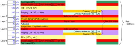
Tip 2: Choose the Right PCB Materials
Dielectric Material
The choice of dielectric material significantly affects the characteristic impedance of a transmission line. The dielectric constant (εr) and the loss tangent (tanδ) are the two key properties to consider. Common PCB dielectric materials include:
| Material | Dielectric Constant (εr) | Loss Tangent (tanδ) |
|---|---|---|
| FR-4 | 4.2 – 4.5 | 0.02 – 0.03 |
| Rogers RO4350B | 3.48 | 0.0037 |
| Isola IS410 | 4.1 | 0.012 |
Copper Thickness and Surface Finish
The thickness of the copper traces and the surface finish also influence the characteristic impedance. Thicker copper traces have lower resistance and inductance, while thinner traces have higher resistance and inductance. Common copper thicknesses for PCBs range from 0.5 oz/ft² to 2 oz/ft².
The surface finish, such as ENIG (Electroless Nickel Immersion Gold) or HASL (Hot Air Solder Leveling), affects the surface roughness and the effective dielectric constant of the transmission line.

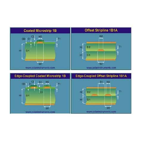
Tip 3: Use Appropriate Trace Geometry
Trace Width and Spacing
The width and spacing of traces on a PCB directly influence the characteristic impedance. Wider traces have lower impedance, while narrower traces have higher impedance. The spacing between traces affects the coupling capacitance and crosstalk.
To achieve a target impedance, use PCB design software or Impedance Calculators to determine the appropriate trace width for a given dielectric material and thickness.
Microstrip vs. Stripline
Microstrip and stripline are two common transmission line geometries used in PCBs.
Microstrip: A microstrip is a trace on the outer layer of a PCB, with a ground plane on the adjacent layer. Microstrips are easier to route and have lower dielectric losses, but they are more susceptible to EMI and have higher radiation losses.
Stripline: A stripline is a trace embedded between two ground planes in the inner layers of a PCB. Striplines have better EMI shielding and lower radiation losses, but they have higher dielectric losses and are more challenging to route.
Coplanar Waveguide (CPW)
A coplanar waveguide is a transmission line geometry where the signal trace and ground planes are on the same layer, with the ground planes parallel to the signal trace. CPWs offer lower dispersion and better isolation compared to microstrips, making them suitable for high-frequency applications.
Tip 4: Minimize Discontinuities
Avoid Abrupt Changes in Impedance
Abrupt changes in the characteristic impedance along a transmission line can cause signal reflections and distortions. To minimize discontinuities:
- Use tapered transitions when changing trace widths
- Avoid sharp bends in traces; use smoothed corners or mitered bends
- Maintain consistent trace width and spacing throughout the signal path
Via Considerations
Vias, which are used to connect traces between layers, can introduce discontinuities and affect the characteristic impedance. To minimize the impact of vias:
- Use smaller via drill sizes and pad diameters
- Place vias strategically to minimize stub lengths
- Consider back-drilling vias to remove unnecessary stub portions
Tip 5: Implement Proper Grounding and Shielding
Ground Planes
Use uninterrupted ground planes on adjacent layers to provide a low-impedance return path for signals. Avoid splitting ground planes unnecessarily, as this can create discontinuities and affect the characteristic impedance.
Stitching Vias
Use stitching vias to connect ground planes on different layers, especially near signal vias. Stitching vias help maintain a continuous ground reference and minimize ground bounce.
Shielding Sensitive Signals
Use shielding techniques to isolate sensitive signals from interference. Techniques include:
- Coplanar shielding: placing ground traces parallel to the signal trace
- Microstrip or stripline shielding: using ground planes above and/or below the signal trace
- Shielded cables or connectors: using shielded interconnects for off-board connections
Tip 6: Consider Differential Signaling
Benefits of Differential Signaling
Differential signaling uses a pair of complementary signals to transmit information, offering several advantages over single-ended signaling:
- Improved noise immunity: differential signals are less susceptible to common-mode noise
- Reduced EMI: differential signals generate less electromagnetic radiation
- Higher signal integrity: differential signals are less affected by ground noise and voltage fluctuations
Differential Impedance
When using differential signaling, the differential impedance (Zdiff) of the trace pair becomes the critical parameter. Differential impedance is influenced by the trace width, spacing, and the coupling between the traces.
To achieve a target differential impedance, use PCB design software or calculators to determine the appropriate trace geometry for the selected dielectric material and thickness.
Tip 7: Simulate and Verify Impedance
Pre-Layout Simulation
Use pre-layout simulation tools to estimate the characteristic impedance of transmission lines based on the PCB stackup and trace geometry. Pre-layout simulations help identify potential impedance mismatches and guide design decisions.
Post-Layout Simulation
After completing the PCB layout, perform post-layout simulations to verify the impedance of critical traces. Post-layout simulations take into account the actual trace geometry, including bends, vias, and other discontinuities.
Time-Domain Reflectometry (TDR)
Use TDR measurements to characterize the impedance profile of transmission lines on a manufactured PCB. TDR measurements help identify impedance discontinuities and validate the impedance control measures implemented in the design.
Tip 8: Collaborate with PCB Manufacturers
Communicate Impedance Requirements
Clearly communicate your impedance requirements to the PCB manufacturer. Provide detailed specifications, including target impedance values, tolerance, and test methods.
Understand Manufacturing Capabilities
Work with the PCB manufacturer to understand their capabilities and limitations in terms of impedance control. Factors to consider include:
- Available dielectric materials and thicknesses
- Minimum trace width and spacing
- Copper thickness and surface finish options
- Impedance testing and measurement capabilities
Incorporate Feedback
Incorporate feedback from the PCB manufacturer during the design process. They can provide valuable insights on design for manufacturability (DFM) and suggest improvements to enhance impedance control.
Tip 9: Implement Controlled Impedance Testing
Test Coupons
Include impedance test coupons on the PCB panel to facilitate controlled impedance testing. Test coupons are small PCB sections that mimic the trace geometry and stackup of critical traces.
Impedance Measurement Techniques
Common impedance measurement techniques include:
- TDR: Time-Domain Reflectometry measures the impedance profile along a transmission line by sending a fast-rise-time pulse and analyzing the reflections.
- VNA: Vector Network Analysis measures the S-parameters of a transmission line, providing information on impedance, loss, and phase characteristics.
Acceptance Criteria
Establish clear acceptance criteria for impedance measurements, specifying the allowable tolerance and the number of test points required. Work with the PCB manufacturer to ensure that the impedance measurements meet the specified criteria.
Tip 10: Document and Learn from Experience
Create Design Guidelines
Develop a set of PCB design guidelines that incorporate best practices for impedance control. These guidelines should cover aspects such as:
- Material selection
- stackup design
- Trace geometry and routing
- Grounding and shielding
- Simulation and verification
Maintain a Knowledge Base
Document the lessons learned from each PCB design project, including successes, challenges, and solutions. Maintain a knowledge base that can be shared within your organization, enabling continuous improvement in impedance control techniques.
Stay Updated with Industry Advancements
Keep abreast of the latest advancements in PCB materials, design tools, and manufacturing processes related to impedance control. Attend conferences, workshops, and webinars to learn from experts and exchange knowledge with peers.
Frequently Asked Questions (FAQ)
-
Q: What is the difference between characteristic impedance and differential impedance?
A: Characteristic impedance (Z0) refers to the impedance of a single transmission line, while differential impedance (Zdiff) refers to the impedance of a pair of coupled transmission lines used for differential signaling. -
Q: How does the dielectric constant of a PCB material affect impedance?
A: The dielectric constant (εr) of a PCB material directly influences the characteristic impedance of a transmission line. A higher dielectric constant results in lower impedance for a given trace geometry. -
Q: What is the purpose of impedance matching?
A: Impedance matching ensures that the characteristic impedance of a transmission line matches the impedance of the source and load. This minimizes signal reflections, reduces distortions, and ensures maximum power transfer. -
Q: How can I minimize the impact of vias on impedance?
A: To minimize the impact of vias on impedance, use smaller via drill sizes and pad diameters, place vias strategically to minimize stub lengths, and consider back-drilling vias to remove unnecessary stub portions. -
Q: What are the benefits of using differential signaling for impedance control?
A: Differential signaling offers improved noise immunity, reduced EMI, and higher signal integrity compared to single-ended signaling. It is less susceptible to common-mode noise, ground noise, and voltage fluctuations.
Conclusion
Effective PCB impedance control is essential for ensuring signal integrity, minimizing EMI, and achieving reliable system performance in high-speed digital and RF applications. By following the ten advanced tips outlined in this article, designers can navigate the complexities of impedance control and make informed decisions throughout the PCB design process.
Key takeaways include:
- Understanding the fundamentals of transmission line theory and impedance matching
- Selecting appropriate PCB materials and trace geometries
- Minimizing discontinuities and implementing proper grounding and shielding techniques
- Considering differential signaling for improved noise immunity and signal integrity
- Simulating, verifying, and testing impedance using pre-layout and post-layout tools, as well as TDR measurements
- Collaborating closely with PCB manufacturers to ensure manufacturability and adherence to impedance requirements
- Documenting design guidelines, maintaining a knowledge base, and staying updated with industry advancements
By mastering these techniques and continually refining their approach, PCB designers can successfully tackle the challenges of impedance control and deliver high-performance, reliable electronic systems.
No responses yet