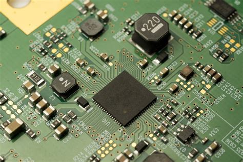
PCB Essentials: Understanding the Fundamentals
Printed Circuit Boards (PCBs) are essential components in modern electronics. They provide a platform for electrical components to be mounted and interconnected, enabling the creation of complex electronic devices. Advanced Circuits is a leading manufacturer of high-quality PCBs, offering a wide range of services and solutions for various industries. In this article, we will explore 10 crucial aspects of Advanced Circuits PCB that every electronics enthusiast, designer, or engineer should know.
1. PCB Materials and Substrates
Advanced Circuits offers a variety of PCB materials and substrates to suit different application requirements. The most common material is FR-4, a glass-reinforced epoxy laminate that offers excellent electrical insulation and mechanical stability. Other materials include:
- High-Frequency Materials (Rogers, Isola)
- Flexible PCBs (Polyimide, Polyester)
- Aluminum PCBs for heat dissipation
- Ceramic PCBs for high-temperature applications
Choosing the right material is crucial for ensuring optimal performance and reliability of your electronic devices.
2. PCB Layers and Thickness
PCBs can be manufactured with various numbers of layers, depending on the complexity of the circuit design. Advanced Circuits offers PCBs with up to 30 layers, allowing for highly intricate and dense designs. The number of layers also affects the overall thickness of the PCB. Standard PCB thicknesses range from 0.8mm to 3.2mm, with thinner boards being more suitable for compact devices and thicker boards offering better mechanical stability.
| Number of Layers | Typical Thickness (mm) |
|---|---|
| 1-2 | 0.8 – 1.6 |
| 4 | 1.6 |
| 6-8 | 1.6 – 2.4 |
| 10-12 | 2.4 – 3.2 |
| 14+ | 3.2+ |
3. PCB Design Software and File Formats
To create PCB designs, engineers and designers use specialized software tools called Electronic Design Automation (EDA) software. Popular EDA software includes:
- Altium Designer
- Cadence OrCAD
- Autodesk Eagle
- KiCad (Open-source)
These software tools allow users to create schematic diagrams, design PCB layouts, and generate manufacturing files. Advanced Circuits accepts various PCB design file formats, including Gerber files (RS-274X), ODB++, and IPC-2581.
4. PCB Fabrication Process
The PCB fabrication process involves several steps to transform a design into a functional printed circuit board. The main steps include:
- PCB Design and Verification
- Film Generation and Printing
- Copper Lamination
- Photoresist Application and Exposure
- Etching and Plating
- Solder Mask Application
- Silkscreen Printing
- Surface Finish Application
- Electrical Testing and Inspection
Advanced Circuits employs state-of-the-art equipment and follows strict quality control procedures to ensure the highest quality PCBs are delivered to their customers.
5. PCB surface finishes
Surface finishes are applied to the exposed copper areas of a PCB to protect them from oxidation and enhance solderability. Advanced Circuits offers several surface finish options, including:
- Hot Air Solder Leveling (HASL)
- Electroless Nickel Immersion Gold (ENIG)
- Immersion Silver (IAg)
- Immersion Tin (ISn)
- Organic Solderability Preservative (OSP)
Each surface finish has its own advantages and limitations, and the choice depends on factors such as the intended application, component types, and environmental conditions.
6. PCB Assembly Options
Advanced Circuits provides both bare PCB manufacturing and PCB assembly services. For assembly, customers can choose between two main options:
- Through-Hole Assembly (THA): Components with leads are inserted through holes in the PCB and soldered on the opposite side.
- Surface Mount Assembly (SMT): Components are mounted directly onto the surface of the PCB using solder paste and reflow soldering.
Advanced Circuits offers various assembly packages, including prototype assembly, partial turnkey assembly, and full turnkey assembly, catering to different customer needs and requirements.
7. PCB testing and Inspection
To ensure the quality and reliability of manufactured PCBs, Advanced Circuits conducts rigorous testing and inspection procedures. These include:
- Automated Optical Inspection (AOI)
- X-Ray Inspection
- In-Circuit Testing (ICT)
- Functional Testing
- Flying Probe Testing
These tests help identify any manufacturing defects, short circuits, open circuits, or component placement issues, ensuring that only high-quality PCBs are delivered to customers.
8. PCB Design Considerations
When designing a PCB, several factors must be considered to ensure optimal performance and manufacturability. These include:
- Component placement and routing
- Signal integrity and electromagneti

No responses yet