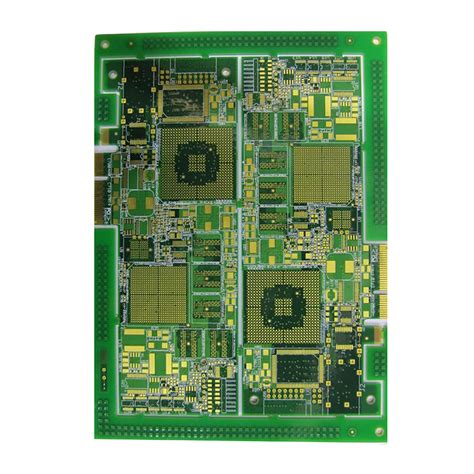
What is HDI PCB?
High Density Interconnect (HDI) PCBs are printed circuit boards with higher wiring density per unit area than conventional PCBs. They have finer lines and spaces, smaller vias, and capture pads, and often contain buried and blind vias. HDI technology allows for denser component placement, enabling the design of smaller, lighter, and more functional electronic products.
Key Features of HDI PCBs
- Fine pitch: HDI PCBs have trace widths and spacings smaller than 100 µm (4 mils).
- Microvias: These are small vias with diameters less than 150 µm (6 mils), allowing for higher density interconnects.
- Buried and blind vias: These vias connect inner layers without going through the entire board thickness, enabling more efficient use of board space.
- High layer count: HDI PCBs often have 8 or more layers to accommodate complex circuitry.
Benefits of Using HDI PCBs
Space Savings
HDI technology allows for the miniaturization of electronic devices by enabling denser component placement and more efficient use of board space. This is particularly important for applications where size and weight are critical factors, such as mobile devices, wearables, and aerospace electronics.
Improved Performance
The shorter signal paths and reduced parasitic capacitance and inductance in HDI PCBs lead to improved signal integrity and reduced electromagnetic interference (EMI). This enables higher signal speeds and better overall performance, making HDI PCBs suitable for high-frequency applications like 5G, radar, and high-speed digital systems.
Enhanced Reliability
HDI PCBs offer enhanced reliability compared to conventional PCBs due to several factors:
- Reduced thermal stress: The smaller vias and traces in HDI PCBs generate less heat, reducing thermal stress on the board.
- Better mechanical stability: The denser interconnect structure provides better mechanical support for components, reducing the risk of solder joint failures.
- Improved power distribution: The increased number of power and ground planes in HDI PCBs enables better power distribution and reduced voltage drop, enhancing overall system reliability.
Cost Effectiveness
Although HDI PCBs have a higher cost per unit area than conventional PCBs, they can be more cost-effective in the long run. The space savings and improved performance offered by HDI technology can reduce the overall system cost by enabling the use of fewer boards, smaller enclosures, and less complex assembly processes.

HDI PCB Manufacturing Process
The HDI PCB manufacturing process involves several key steps:
-
Material selection: HDI PCBs typically use high-performance substrates like polyimide or high-Tg FR-4 to ensure better thermal and mechanical stability.
-
Lamination: The core layers are laminated together using high-pressure and temperature, forming a solid board.
-
Drilling: Mechanical or laser drilling is used to create through holes, blind vias, and buried vias in the board.
-
Plating: The drilled holes are plated with copper to establish electrical connections between layers.
-
Patterning: The desired circuit pattern is transferred onto the board using photolithography and etching processes.
-
Solder mask application: A solder mask is applied to protect the copper traces and prevent short circuits.
-
Surface finish: A surface finish, such as ENIG (Electroless Nickel Immersion Gold) or HASL (Hot Air Solder Leveling), is applied to the exposed copper pads to improve solderability and protect against oxidation.
-
Electrical testing: The finished HDI PCB undergoes rigorous electrical testing to ensure functionality and reliability.

Choosing the Right HDI PCB Manufacturer
When selecting an HDI PCB manufacturer, consider the following factors:
-
Technical capabilities: Ensure that the manufacturer has the necessary equipment, expertise, and experience to produce high-quality HDI PCBs.
-
Quality control: Look for a manufacturer with a robust quality management system, such as ISO 9001 certification, and a track record of delivering consistent, reliable products.
-
Customer support: Choose a manufacturer that offers excellent customer support, including responsive communication, technical assistance, and timely issue resolution.
-
Turnaround time: Consider the manufacturer’s lead times and ability to meet your project deadlines.
-
Cost: While cost is an important factor, it should not be the sole deciding factor. Prioritize manufacturers that offer a balance of quality, reliability, and competitive pricing.

HDI PCB Design Considerations
When designing HDI PCBs, keep the following considerations in mind:
-
Design rules: Adhere to the manufacturer’s HDI design rules, including minimum trace widths, spacings, and via sizes, to ensure manufacturability and reliability.
-
Signal integrity: Use appropriate layout techniques, such as controlled impedance routing and proper termination, to maintain signal integrity and minimize EMI.
-
Thermal management: Consider the thermal requirements of your components and incorporate adequate thermal relief and heat dissipation features in your HDI PCB design.
-
Testability: Design your HDI PCB with testability in mind, incorporating test points and other features that facilitate automated optical inspection (AOI) and electrical testing.
Applications of HDI PCBs
HDI PCBs find applications in a wide range of industries and products, including:
- Consumer electronics: Smartphones, tablets, wearables, and IoT devices.
- Automotive electronics: Advanced driver assistance systems (ADAS), infotainment systems, and electric vehicle power electronics.
- Medical devices: Implantable devices, diagnostic equipment, and wearable health monitors.
- Aerospace and defense: Avionics, radar systems, and satellite communication equipment.
- Industrial automation: Robotics, machine vision systems, and process control equipment.
Comparing HDI PCBs with Conventional PCBs
| Parameter | HDI PCBs | Conventional PCBs |
|---|---|---|
| Trace width/spacing | <100 µm (4 mils) | >100 µm (4 mils) |
| Via diameter | <150 µm (6 mils) | >150 µm (6 mils) |
| Layer count | Typically 8 or more | Typically fewer than 8 |
| Board size | Smaller | Larger |
| Component density | Higher | Lower |
| Signal integrity | Better | Good |
| Cost per unit area | Higher | Lower |
Future Trends in HDI PCB Technology
As electronic devices continue to become smaller, more powerful, and more interconnected, HDI PCB technology is expected to evolve to meet these demands. Some future trends in HDI PCB technology include:
-
Finer features: The industry will continue to push for finer trace widths, spacings, and via sizes to enable even denser PCB designs.
-
Advanced materials: The adoption of advanced substrate materials, such as low-loss dielectrics and high-thermal-conductivity laminates, will enable better signal integrity and thermal management in HDI PCBs.
-
Embedded components: The integration of passive components, such as resistors and capacitors, directly into the PCB substrate will further increase component density and reduce board size.
-
3D packaging: The use of 3D packaging techniques, such as package-on-package (PoP) and system-in-package (SiP), will enable the creation of highly integrated, multi-functional modules using HDI PCBs.
-
Additive manufacturing: The growing interest in additive manufacturing techniques, such as 3D printing, for PCB fabrication may lead to new possibilities for HDI PCB design and production.
Frequently Asked Questions (FAQ)
1. What is the minimum trace width and spacing achievable with HDI PCBs?
The minimum trace width and spacing in HDI PCBs can be as small as 50 µm (2 mils), depending on the manufacturer’s capabilities and the specific design requirements. However, most HDI PCBs have trace widths and spacings between 75 µm (3 mils) and 100 µm (4 mils).
2. How do HDI PCBs handle high-speed signals compared to conventional PCBs?
HDI PCBs offer better signal integrity for high-speed signals compared to conventional PCBs. The shorter signal paths, reduced parasitic capacitance and inductance, and more uniform impedance control in HDI PCBs help minimize signal distortion, reflection, and crosstalk. This makes HDI PCBs suitable for high-frequency applications like 5G, radar, and high-speed digital systems.
3. Are HDI PCBs more expensive than conventional PCBs?
Yes, HDI PCBs generally have a higher cost per unit area than conventional PCBs due to the more advanced manufacturing processes and materials required. However, the space savings and improved performance offered by HDI technology can reduce the overall system cost by enabling the use of fewer boards, smaller enclosures, and less complex assembly processes, making them cost-effective in the long run.
4. What are the typical applications of HDI PCBs?
HDI PCBs find applications in a wide range of industries and products where high component density, small form factors, and high-performance are required. Some typical applications include smartphones, tablets, wearables, IoT devices, automotive electronics, medical devices, aerospace and defense systems, and industrial automation equipment.
5. How can I ensure the manufacturability and reliability of my HDI PCB design?
To ensure the manufacturability and reliability of your HDI PCB design, follow these best practices:
- Adhere to the manufacturer’s HDI design rules and guidelines.
- Use appropriate layout techniques to maintain signal integrity and minimize EMI.
- Consider the thermal requirements of your components and incorporate adequate thermal management features.
- Design your HDI PCB with testability in mind, incorporating test points and features that facilitate automated inspection and testing.
- Work closely with your HDI PCB manufacturer throughout the design and production process to address any issues and optimize your design for manufacturing.
By partnering with a reliable and experienced HDI PCB manufacturer and following these best practices, you can ensure the successful development and production of your HDI PCB-based products.
No responses yet