
What is PCB Silkscreen?
PCB silkscreen, also known as legend or nomenclature, is a layer of text and symbols printed on the surface of a printed circuit board (PCB). The silkscreen layer provides essential information about the components, their placement, and the overall layout of the board. This information is crucial for assembly, debugging, and maintenance purposes.
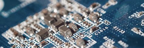
The silkscreen layer is typically printed using a white or yellow ink, although other colors may be used depending on the PCB’s color and design requirements. The ink is applied using a screen-printing process, which involves forcing the ink through a fine mesh screen onto the PCB surface.
Importance of PCB Silkscreen
PCB silkscreen serves several important functions:
-
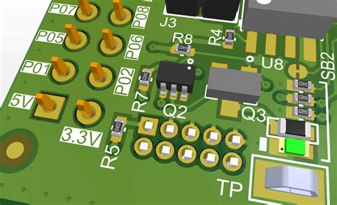
Component Identification: Silkscreen labels help identify components, such as resistors, capacitors, and integrated circuits (ICs), by providing their reference designators (e.g., R1, C2, U3). This information is essential for assembly and troubleshooting.
-
Orientation Marking: Silkscreen can indicate the proper orientation of components, such as polarized capacitors, diodes, and ICs, using symbols like dots, notches, or arrows.
-
Test Points: Silkscreen can mark test points on the PCB, which are used for probing and debugging purposes.
-
Branding and Aesthetics: Silkscreen can include company logos, product names, and other branding elements to enhance the overall appearance of the PCB.
Designing PCB Silkscreen
When designing PCB silkscreen, there are several best practices to follow:
Font and Size
Choose a clear, legible font for your silkscreen text. Sans-serif fonts like Arial or Helvetica are popular choices. The font size should be large enough to be easily readable, typically at least 0.8mm (0.032 inches) in height.
Placement
Silkscreen text and symbols should be placed in a way that does not interfere with component placement or soldering. Avoid placing silkscreen on top of pads or traces, as this can lead to problems during assembly and soldering.
Alignment
Align silkscreen text and symbols consistently throughout the PCB design. For example, component reference designators should be placed in the same relative position for each component type (e.g., above and to the left of each resistor).
Clarity and Contrast
Ensure that the silkscreen is clearly visible against the background color of the PCB. If the PCB has a dark solder mask, use white or light-colored silkscreen ink for better contrast. Conversely, if the PCB has a light-colored solder mask, use black or dark-colored ink.
Silkscreen Elements
Some common elements found in PCB silkscreen include:
| Element | Description |
|---|---|
| Reference Designators | Unique identifiers for each component (e.g., R1, C2, U3) |
| Component Outlines | Simplified outlines of components to indicate their placement |
| Orientation Markers | Dots, notches, or arrows to indicate component orientation |
| Test Points | Labeled points for probing and debugging |
| Logos and Branding | Company logos, product names, and other branding elements |
PCB Silkscreen Manufacturing Process
The PCB silkscreen manufacturing process involves several steps:
-
Screen Preparation: A fine mesh screen is coated with a light-sensitive emulsion and exposed to UV light through a film positive of the silkscreen artwork. The exposed areas harden, while the unexposed areas remain soft and are washed away, creating a stencil of the silkscreen design.
-
Ink Application: The prepared screen is placed over the PCB, and ink is applied to the screen using a squeegee. The ink is forced through the open areas of the stencil onto the PCB surface.
-
Curing: After the ink is applied, the PCB is heated to cure the ink and ensure proper adhesion to the board surface.
-
Inspection: The finished PCB is inspected to ensure that the silkscreen is clear, accurate, and properly aligned with the components and features of the board.

Common PCB Silkscreen Mistakes and How to Avoid Them
-
Incorrect Component Placement: Double-check the placement of components and their corresponding silkscreen labels to ensure they match the schematic and layout.
-
Overlapping Silkscreen and Pads: Ensure that silkscreen elements do not overlap with component pads or traces, as this can lead to assembly and soldering issues.
-
Unreadable Text: Use a clear, legible font with sufficient size to ensure that silkscreen text is easily readable.
-
Inconsistent Alignment: Maintain consistent alignment of silkscreen elements throughout the PCB design for a professional appearance and easier readability.
-
Poor Contrast: Choose silkscreen ink colors that provide good contrast against the PCB background color to ensure clear visibility.
FAQ
-
Q: Can PCB silkscreen be applied to both sides of the board?
A: Yes, silkscreen can be applied to both the top and bottom sides of a PCB, depending on the design requirements. -
Q: Is it possible to have multiple colors of silkscreen on a single PCB?
A: While most PCBs use a single color for silkscreen (typically white or yellow), it is possible to use multiple colors. However, this may increase the complexity and cost of the manufacturing process. -
Q: Can silkscreen be used on flexible PCBs?
A: Yes, silkscreen can be applied to flexible PCBs, but the ink and curing process may differ from that used for rigid PCBs to ensure compatibility with the flexible substrate. -
Q: How durable is PCB silkscreen?
A: PCB silkscreen is generally durable and resistant to wear and abrasion. However, it can be damaged by harsh chemicals or excessive mechanical stress. -
Q: Can silkscreen be removed or modified after the PCB has been manufactured?
A: Removing or modifying silkscreen after manufacturing is difficult and not recommended, as it may damage the PCB surface or components. It is best to ensure that the silkscreen design is correct before manufacturing.
Conclusion
PCB silkscreen is an essential element of PCB design, providing critical information for assembly, debugging, and maintenance. By following best practices for silkscreen design and understanding the manufacturing process, you can ensure that your PCBs are clearly labeled, easy to assemble, and professional in appearance. Avoid common mistakes, such as incorrect component placement, overlapping silkscreen and pads, and poor contrast, to create high-quality PCBs that meet your design requirements.
No responses yet