Introduction to Gerber Files in PCB Design
Gerber files are the standard file format used in the PCB (Printed Circuit Board) design industry for manufacturing purposes. They contain all the necessary information required to fabricate a PCB, including the copper layers, solder mask, silkscreen, and drill data. Understanding Gerber file extensions is crucial for PCB designers to ensure that their designs are accurately translated into physical boards.
What are Gerber Files?
Gerber files, named after the Gerber Scientific Instrument Company, are a set of vector-based file formats used to describe the various layers of a PCB. These files are generated by PCB design software and are used by PCB manufacturers to create the physical boards. Each Gerber file represents a specific layer or aspect of the PCB, such as the copper traces, solder mask, or drill holes.
Why are Gerber Files Important in PCB Design?
Gerber files play a critical role in the PCB design and manufacturing process. They serve as the bridge between the designer’s vision and the manufacturer’s production capabilities. By providing a standardized format for conveying PCB design information, Gerber files ensure that the manufactured board accurately reflects the designer’s intentions. They also enable efficient communication between designers and manufacturers, reducing the likelihood of errors and misinterpretations.
Common Gerber File Extensions
There are several Gerber file extensions used in PCB design, each representing a specific layer or aspect of the board. Here are some of the most common Gerber file extensions:
1. .GTL – Top Copper Layer
The .GTL file extension represents the top copper layer of the PCB. It contains the copper traces and pads on the top side of the board. This layer is responsible for connecting components and routing signals on the top surface of the PCB.
2. .GBL – Bottom Copper Layer
The .GBL file extension represents the bottom copper layer of the PCB. It contains the copper traces and pads on the bottom side of the board. This layer is used for routing signals and connecting components on the bottom surface of the PCB.
3. .GTO – Top Overlay Layer
The .GTO file extension represents the top overlay layer, also known as the silkscreen layer. It contains the text, logos, and component outlines printed on the top side of the PCB. This layer aids in component placement and provides visual information for assembly and debugging purposes.
4. .GBO – Bottom Overlay Layer
The .GBO file extension represents the bottom overlay layer, similar to the top overlay layer but for the bottom side of the PCB. It contains the silkscreen information printed on the bottom surface of the board.
5. .GTS – Top Solder Mask Layer
The .GTS file extension represents the top solder mask layer. It defines the areas on the top side of the PCB where the solder mask should be applied. The solder mask is a protective coating that prevents accidental short circuits and helps in soldering components to the board.
6. .GBS – Bottom Solder Mask Layer
The .GBS file extension represents the bottom solder mask layer, similar to the top solder mask layer but for the bottom side of the PCB.
7. .GTP – Top Paste Layer
The .GTP file extension represents the top paste layer, also known as the solder paste layer. It defines the areas on the top side of the PCB where solder paste should be applied for surface mount components. Solder paste is a mixture of tiny solder particles and flux that helps in the soldering process.
8. .GBP – Bottom Paste Layer
The .GBP file extension represents the bottom paste layer, similar to the top paste layer but for the bottom side of the PCB.
9. .TXT – Drill File
The .TXT file extension is used for the drill file, which contains information about the location, size, and type of drill holes on the PCB. This file is essential for creating the holes required for through-hole components and vias.
Here’s a table summarizing the common Gerber file extensions:
| Extension | Layer Description |
|---|---|
| .GTL | Top Copper Layer |
| .GBL | Bottom Copper Layer |
| .GTO | Top Overlay (Silkscreen) Layer |
| .GBO | Bottom Overlay (Silkscreen) Layer |
| .GTS | Top Solder Mask Layer |
| .GBS | Bottom Solder Mask Layer |
| .GTP | Top Paste (Solder Paste) Layer |
| .GBP | Bottom Paste (Solder Paste) Layer |
| .TXT | Drill File |

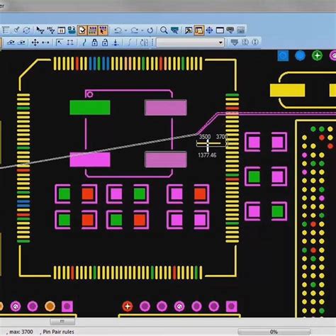
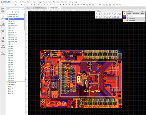
Generating Gerber Files in PCB Design Software
Most PCB design software, such as Altium Designer, KiCad, or Eagle, have built-in functionality to generate Gerber files. The process of generating Gerber files typically involves the following steps:
- Complete the PCB design, ensuring that all layers and components are correctly placed and routed.
- Set up the Gerber file output settings, specifying the desired file format, resolution, and aperture settings.
- Select the layers to be included in the Gerber files, such as the copper layers, solder mask, silkscreen, and drill data.
- Generate the Gerber files, which will create a set of files with the appropriate extensions for each layer.
- Review the generated Gerber files to ensure accuracy and completeness.
It’s important to consult the documentation or tutorials specific to your PCB design software for detailed instructions on generating Gerber files.

Best Practices for Working with Gerber Files
To ensure smooth communication with PCB manufacturers and minimize the chances of errors, consider the following best practices when working with Gerber files:
- Use a consistent naming convention for your Gerber files to avoid confusion and make it easier for manufacturers to identify the layers.
- Include all necessary layers in the Gerber file set, such as copper layers, solder mask, silkscreen, and drill data.
- Verify the accuracy of your Gerber files by using a Gerber viewer or online Gerber file checker before sending them to the manufacturer.
- Provide clear instructions and specifications to the manufacturer, including any special requirements or preferences for the PCB fabrication process.
- Communicate openly with the manufacturer and be prepared to answer any questions or provide additional information if needed.
By following these best practices, you can streamline the PCB manufacturing process and ensure that your designs are accurately translated into physical boards.
FAQ
-
What is the difference between Gerber files and other PCB design files?
Gerber files are a standard file format used specifically for PCB manufacturing. They contain all the necessary information required to fabricate a PCB, including the copper layers, solder mask, silkscreen, and drill data. Other PCB design files, such as schematic files or layout files, are used during the design process but are not directly used for manufacturing. -
Can I view Gerber files without special software?
While Gerber files are not easily readable by humans, there are specialized Gerber viewer software and online tools available that allow you to view and analyze Gerber files. These tools help in verifying the accuracy of the Gerber files before sending them to the manufacturer. -
What happens if I miss a layer in the Gerber files?
If you miss a layer in the Gerber files, such as forgetting to include the solder mask or drill data, it can lead to manufacturing issues. The PCB manufacturer may not be able to produce the board accurately without all the necessary layers. It’s crucial to double-check that all required layers are included in the Gerber file set before submitting them for manufacturing. -
Can I use different file extensions for Gerber files?
While the standard Gerber file extensions are widely recognized and accepted by PCB manufacturers, it’s possible to use different file extensions as long as they are clearly communicated to the manufacturer. However, it’s recommended to stick to the standard extensions to avoid confusion and ensure compatibility with the manufacturer’s systems. -
How do I ensure the accuracy of my Gerber files?
To ensure the accuracy of your Gerber files, you can follow these steps: - Double-check your PCB design for any errors or inconsistencies before generating the Gerber files.
- Use a Gerber viewer or online Gerber file checker to visually inspect the generated files for any issues.
- Verify that all necessary layers are included in the Gerber file set.
- Provide clear instructions and specifications to the manufacturer to avoid misinterpretations.
- Communicate openly with the manufacturer and be prepared to answer any questions or provide additional clarifications if needed.
Conclusion
Understanding Gerber file extensions is essential for PCB designers to ensure accurate and efficient communication with PCB manufacturers. Gerber files serve as the standard format for conveying PCB design information, including the copper layers, solder mask, silkscreen, and drill data. By familiarizing yourself with the common Gerber file extensions and following best practices for working with Gerber files, you can streamline the PCB manufacturing process and avoid potential errors.
Remember to generate complete and accurate Gerber files from your PCB design software, include all necessary layers, and provide clear instructions to the manufacturer. By doing so, you can bridge the gap between your design vision and the physical realization of your PCB.
No responses yet